DIRECT INK WRITING PRINTER
NOVA Materials Dispensing System
DIRECT INK WRITING PRINTER
NOVA Materials Dispensing System
Unlock new opportunities and accelerate research and development with this additive manufacturing printer using a range of functional materials and screen-printable inks.
Price: Contact sales to configure NOVA
Meet NOVA — a materials dispensing system

Streamline research and development
Change circuit designs on the fly and get immediate feedback on new ideas, accelerating R&D in advanced materials and flexible hybrid electronics.

Total material freedom
Experiment with a wide range of high-performance materials and seamlessly transition to mass production using screen printing.

Flexible form factors
Stack multiple layers on flexible, stretchable, soft, or conformable substrates to make wearables, soft robotics, medical sensors, and more.

Clear workflows for consistent result
Guided steps make it easy for different users to run the same process reliably, ensuring continuity and repeatability despite turnover or role changes.
NOVA APPLICATIONS
What NOVA prints

MULTILAYER PRINTING
Working with NOVA's software
NOVA offers features such as multilayer printing and the ability to alter the sequence of trace printing.
- •Print up to 4 stack-up layers (multiple materials can be assigned to each layer)
- •Perform multilayer and multimaterial printing
- •Edit print jobs in a single workflow
- •Minimize setup time for repeat print jobs
MULTILAYER PRINTING
Printed sensors: University of Waterloo
“My research involves developing flexible and stretchable sensors for wearable electronics. With the Plan feature, I can separate different sensor elements, traces, or components to different layers and remove toolpaths that I don't want. The ability to change the direction of tool paths has helped me the most — there's no air pockets, and I have a very uniform trace width because I started printing in a designated safe region.”
– Nick Levinski, University of Waterloo

VOLTERA'S PRINTING SERVICE
Need us to print your prototypes?
Submit your designs. We'll print them on NOVA and ship them to you.
VOLTERA'S PRINTING SERVICE
Need us to print your prototypes?
Submit your designs. We'll print them on NOVA and ship them to you.


BENEFITS
Innovate without limits
Streamline research and development with a direct ink writing printer

No tooling
Change designs on the fly and iterate without screens or stencils, eliminating delays and reducing costs.
No waste
Print only what's needed, conserving valuable material.
No cleanup
Material is contained throughout the printing process, simplifying cleaning and handling procedures.
90% faster
Iteration time96% reduced
Material costsExplore new possibilities with high resolution materials dispensing

Wide material options
Our material dispensing system is compatible with a wide range of viscosities from inks to pastes, ensuring high conductivity, solderability, and energy density.
Seamless scalability
Validate designs and materials in the lab and seamlessly transition into production with scalable printing technologies.
Repeatable results
Achieve repeatable results with closed-loop pressure feedback, temp-controlled dispensing, and an optimized algorithm for multilayer printing.
100 µm
Line width [1]1,000 - 1,000,000 cP
Viscosity range≥107 S/m
Conductivity (single pass)Adapt to most substrates with a large, configurable print area
Rigid substrates
Secure your rigid substrates like glass and ceramic of various shapes and sizes with provided threads onto the mounting grid.
Compliant substrates
Secure your conformable substrates like TPU with NOVA's porous titanium vacuum table, which applies uniform suction.
Unconventional substrates
Develop application-specific fixturing for unconventional substrates using the mounting grid features.
220 mm × 300 mm
Print area40 mm × 40 mm, M5
Mounting gridEnsure print accuracy with integrated computer vision

Eliminate registration errors
Accurately position and align patterns with augmented reality overlay.
Optimize print quality
Find the ideal height, pressure, and print settings with a dedicated material calibration workflow.
Simplify reporting
Capture images for analysis, measurements, and documentation.
17 µm/pixel
Camera resolution [2]1920 × 1080
Image sizeProtect intellectual property with easy-to-use software

Offline mode supported
Protect your IP by operating offline via a direct Ethernet connection.
Smooth onboarding
Guided workflows, walk-through videos, and user profiles in the browser-based app set you up for success.
Seamless cooperation and independent research
Browse, create, and modify saved profiles for materials and substrates with the central materials library.
In-app access to support
Gerber file compatible
Up to 4
Stack-up layers [3]Streamline research and development with a direct ink writing printer
No tooling
Change designs on the fly and iterate without screens or stencils, eliminating delays and reducing costs.
No waste
Print only what's needed, conserving valuable material.
No cleanup
Material is contained throughout the printing process, simplifying cleaning and handling procedures.
90% faster
Iteration time96% reduced
Material costsExplore new possibilities with high resolution materials dispensing
Wide material options
Our material dispensing system is compatible with a wide range of viscosities from inks to pastes, ensuring high conductivity, solderability, and energy density.
Seamless scalability
Validate designs and materials in the lab and seamlessly transition into production with scalable printing technologies.
Repeatable results
Achieve repeatable results with closed-loop pressure feedback, temp-controlled dispensing, and an optimized algorithm for multilayer printing.
100 µm
Line width [1]1,000 - 1,000,000 cP
Viscosity range≥107 S/m
Conductivity (single pass)Adapt to most substrates with a large, configurable print area
Rigid substrates
Secure your rigid substrates like glass and ceramic of various shapes and sizes with provided threads onto the mounting grid.
Compliant substrates
Secure your conformable substrates like TPU with NOVA's porous titanium vacuum table, which applies uniform suction.
Unconventional substrates
Develop application-specific fixturing for unconventional substrates using the mounting grid features.
220 mm × 300 mm
Print area40 mm × 40 mm, M5
Mounting gridEnsure print accuracy with integrated computer vision
Eliminate registration errors
Accurately position and align patterns with augmented reality overlay.
Optimize print quality
Find the ideal height, pressure, and print settings with a dedicated material calibration workflow.
Simplify reporting
Capture images for analysis, measurements, and documentation.
17 µm/pixel
Camera resolution [2]1920 × 1080
Image sizeProtect intellectual property with easy-to-use software
Offline mode supported
Protect your IP by operating offline via a direct Ethernet connection.
Smooth onboarding
Guided workflows, walk-through videos, and user profiles in the browser-based app set you up for success.
Seamless cooperation and independent research
Browse, create, and modify saved profiles for materials and substrates with the central materials library.
In-app access to support
Gerber file compatible
Up to 4
Stack-up layers [3]HARDWARE
Anatomy of NOVA

NOVA


Who's using NOVA


TESTIMONIALS
What customers say about NOVA
York University
“I think where this sort of technology, NOVA, will shine is in applications that were not possible before. You shouldn't fight or try to compete with, you know, silicon chips or PCBs. You should try to make something that's impossible with those technologies.”
– Gerd Grau, Director of the Electronics Additive Manufacturing Lab at York University
MIT
“What we've been able to do with NOVA is print carbon nanotube inks and get field-emitted electrons. (...) Working with NOVA has been fascinating. We've been able to construct devices that we would not be able to do conventionally without expending enormous time and resources.”
– Alex Kashkin, Graduate Researcher, Velásquez Group at MIT
ACI Materials
“I've printed frequently with NOVA and use it to develop characterization techniques for further product development for us. NOVA is very different from any other product. I would say the user interface is very friendly. It's the type of machine that I would feel comfortable handing off to technicians.”
– Andrew Bambach, Production Manager at ACI
CUSTOMER STORIES
See what others are doing with NOVA
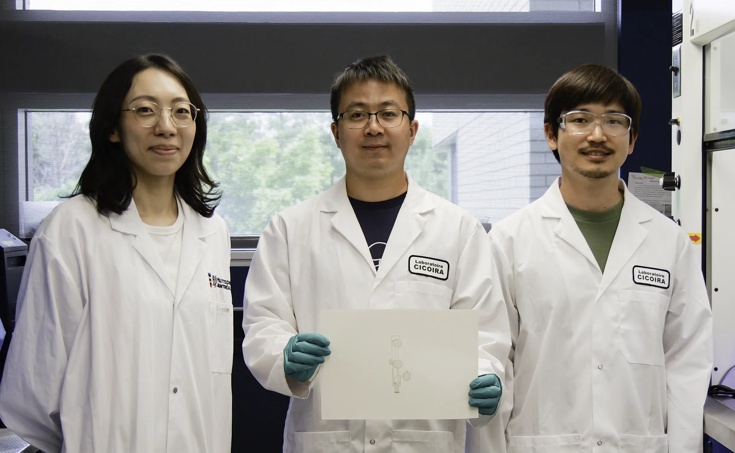
Polytechnique Montréal
Print Stretchable Bioelectronics for Research with NOVA
Professor Fabio Cicoira and his team at Polytechnique Montréal utilize NOVA and V-One to develop flexible and stretchable organic bioelectronics.
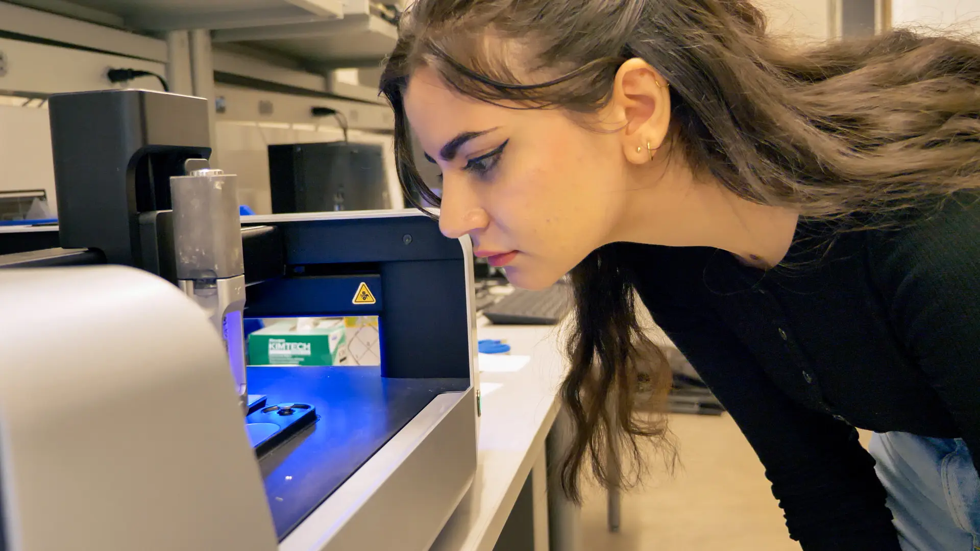
York University
Advance Electronics Additive Manufacturing with Voltera
V-One was a staple at York University’s Electronics Additive Manufacturing Lab. Then, in 2022, they leveled up their lab by adding a NOVA.
PUBLICATIONS
NOVA in academic research
- [1]
D Dye, A Schmidt, M Cozzens, Development of a Modular Solar Shingle, 2024, ideaexchange.uakron.edu
- [2]
D Lagace, C Shafai, A Stretchable Extrusion Printed Piezoresistive Strain Sensor for Respiration Monitoring, 2024, ieeexplore.ieee.org
- [3]
D Lagace, A Study of Extrusion Printed Millimetre-Scale MEMS Transducers, 2025, mspace.lib.umanitoba.ca
- [4]
D Lagace, T Chen, C Shafai, An extrusion printed capacitively interrogated DC electric field sensor, 2024, ieeexplore.ieee.org
- [5]
B Ybarra, Impact of Post-Processing on Electrical Conductivity of 3D Printed Thin Films, 2024, scholarworks.calstate.edu
- [6]
E Reese, B Daniels, Smart Insole Prototype Development, 2025, exhibit.xavier.edu
- [7]
S Patel, V Porcila, AM Alvaran, J Nugara…, Designing Silver Conductive Ink S-Curve Interconnects for Bio-potential Monitoring E-Textiles Via Material Deposition Fabrication, 2025, computer.org
- [8]
A Gohel, M Gratuze, M Ketabi, R Izquierdo, Direct-write printing for flexible and 3D electronics: Aerosol jet vs. Micro dispensing, 2025, mdpi.com
- [9]
J Abounasr, M El Gharbi, RF García…, Design and Fabrication of a Biocompatible Antenna for Wearable Technologies, 2025, ieeexplore.ieee.org
- [10]
A Kachkine… , Densely packed, additively manufactured, in-plane gated carbon nanotube field emission electron sources, 2022, ieeexplore.ieee.org
PUBLICATIONS
NOVA in academic research
- [1]
D Dye, A Schmidt, M Cozzens, Development of a Modular Solar Shingle, 2024, ideaexchange.uakron.edu
- [2]
D Lagace, C Shafai, A Stretchable Extrusion Printed Piezoresistive Strain Sensor for Respiration Monitoring, 2024, ieeexplore.ieee.org
- [3]
D Lagace, A Study of Extrusion Printed Millimetre-Scale MEMS Transducers, 2025, mspace.lib.umanitoba.ca
- [4]
D Lagace, T Chen, C Shafai, An extrusion printed capacitively interrogated DC electric field sensor, 2024, ieeexplore.ieee.org
- [5]
B Ybarra, Impact of Post-Processing on Electrical Conductivity of 3D Printed Thin Films, 2024, scholarworks.calstate.edu
- [6]
E Reese, B Daniels, Smart Insole Prototype Development, 2025, exhibit.xavier.edu
- [7]
S Patel, V Porcila, AM Alvaran, J Nugara…, Designing Silver Conductive Ink S-Curve Interconnects for Bio-potential Monitoring E-Textiles Via Material Deposition Fabrication, 2025, computer.org
- [8]
A Gohel, M Gratuze, M Ketabi, R Izquierdo, Direct-write printing for flexible and 3D electronics: Aerosol jet vs. Micro dispensing, 2025, mdpi.com
- [9]
J Abounasr, M El Gharbi, RF García…, Design and Fabrication of a Biocompatible Antenna for Wearable Technologies, 2025, ieeexplore.ieee.org
- [10]
A Kachkine… , Densely packed, additively manufactured, in-plane gated carbon nanotube field emission electron sources, 2022, ieeexplore.ieee.org
FAST FACTS
Frequently asked questions
For U.S. customers: NOVA is made in Canada and is exempt from U.S. tariffs under the USMCA trade agreement. This may change without notice if there are updates to import policies. For more information on U.S. imposed tariffs, visit whitehouse.gov.
Specs for the NOVA materials dispensing system:
- Dimensions: 675 × 605 × 345 mm
- Weight: ~35 kg
- Power: 100–240 VAC, 50/60 Hz, 221 W
- Connectivity: USB-A 2.0/3.0, Ethernet, Wi-Fi (dongle included)
- Motion/precision: XYZ resolution 2.5 µm × 7 µm × 1.25 µm; ± 20 µm stated accuracy
- Temperature control: up to 40 °C (material)
- Syringe capacity: up to 2.5 mL
NOVA is a direct ink writing machine that micro-dispenses on flexible, stretchable, soft, and rigid substrates to fit your use case.
Yes. NOVA can be used as an adhesive dispensing system for electronics R&D, delivering controlled bead/line placement with micron-scale accuracy. See our adhesive dispensing page for more information.
Yes. NOVA functions as a flexible electronics printer that holds thin films and fabrics flat with a vacuum table and maps height for consistent deposition. It supports flexible material dispensing on PET, polyimide (Kapton), TPU, and textiles, and teams building wearables often treat it like a soft electronics printer.
Yes. As a conductive ink printer, NOVA lays down uniform lines for RF antennas, strain/pressure sensors, and flexible circuitry using silver, copper, carbon, or functional ink(s).
NOVA accepts standard Gerber files; SVG format is also supported, though it’s currently a beta feature. The browser-based app seamlessly fits into your existing ECAD workflows by supporting standard design output formats, and the NOVA documentation includes setup and usage instructions provided freely online, so you can prepare files correctly from day one.
With Plan, you can assign multiple materials across up to four stack-up layers, reorder toolpaths, and save repeat jobs. Teams commonly stack conductor, dielectric, and adhesive layers, using high-viscosity inks and viscoelastic inks for true multimaterial printing.
For U.S. customers: NOVA is made in Canada and is exempt from U.S. tariffs under the USMCA trade agreement. This may change without notice if there are updates to import policies. For more information on U.S. imposed tariffs, visit whitehouse.gov.
Yes. NOVA can be used as an adhesive dispensing system for electronics R&D, delivering controlled bead/line placement with micron-scale accuracy. See our adhesive dispensing page for more information.
Yes. As a conductive ink printer, NOVA lays down uniform lines for RF antennas, strain/pressure sensors, and flexible circuitry using silver, copper, carbon, or functional ink(s).
With Plan, you can assign multiple materials across up to four stack-up layers, reorder toolpaths, and save repeat jobs. Teams commonly stack conductor, dielectric, and adhesive layers, using high-viscosity inks and viscoelastic inks for true multimaterial printing.
Specs for the NOVA materials dispensing system:
- Dimensions: 675 × 605 × 345 mm
- Weight: ~35 kg
- Power: 100–240 VAC, 50/60 Hz, 221 W
- Connectivity: USB-A 2.0/3.0, Ethernet, Wi-Fi (dongle included)
- Motion/precision: XYZ resolution 2.5 µm × 7 µm × 1.25 µm; ± 20 µm stated accuracy
- Temperature control: up to 40 °C (material)
- Syringe capacity: up to 2.5 mL
NOVA is a direct ink writing machine that micro-dispenses on flexible, stretchable, soft, and rigid substrates to fit your use case.
Yes. NOVA functions as a flexible electronics printer that holds thin films and fabrics flat with a vacuum table and maps height for consistent deposition. It supports flexible material dispensing on PET, polyimide (Kapton), TPU, and textiles, and teams building wearables often treat it like a soft electronics printer.
NOVA accepts standard Gerber files; SVG format is also supported, though it’s currently a beta feature. The browser-based app seamlessly fits into your existing ECAD workflows by supporting standard design output formats, and the NOVA documentation includes setup and usage instructions provided freely online, so you can prepare files correctly from day one.

GET A DEMONSTRATION
Want to see NOVA in action?
NOVA is the electronics printer that will help bridge the gap between what you can do and what you wish you could do with electronics. Take a look at how people are using NOVA for rapid prototyping of additive electronic devices and to print electronics on everything.