White paper
Printing Electroluminescent Ink on Paper and PET
Due to their consistent brightness, low cost and high energy efficiency, electroluminescent inks are used in a wide range of electroluminescent display applications. This project is an example of printing an electroluminescent ink on soft and flexible substrates.


- Polyethylene terephthalate (PET)
- Cardstock paper
Video
Project overview
Purpose
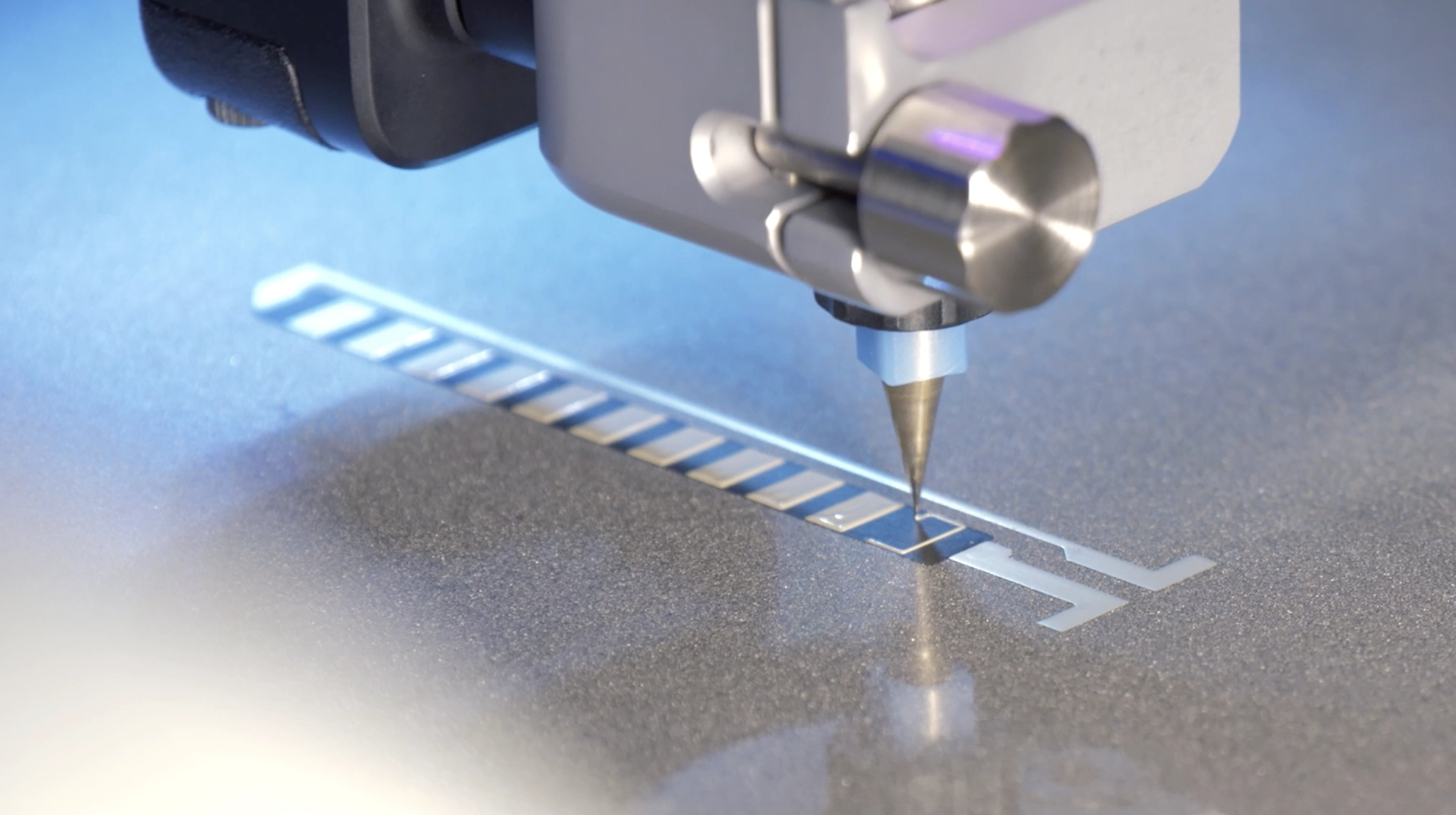
The purpose of this project was to demonstrate the multilayer capability of Voltera NOVA. We printed a blue light-emitting pattern — the Voltera logo — on two substrates: paper and PET separately, using electroluminescent ink.

Design layout
Electroluminescence operates by exciting a phosphor material with an electric field. An inverter is needed to convert the direct current from the power source into alternating current.
Based on this mechanism, our design positions a phosphor layer between two conductive layers, incorporating a dielectric ink layer to insulate the phosphor. The printing sequence is as follows:
- Layer 1: Base conductive layer
- Layer 2: Dielectric layer
- Layer 3: Phosphor layer
- Layer 4: Top conductive layer
Layer overview

Desired outcome
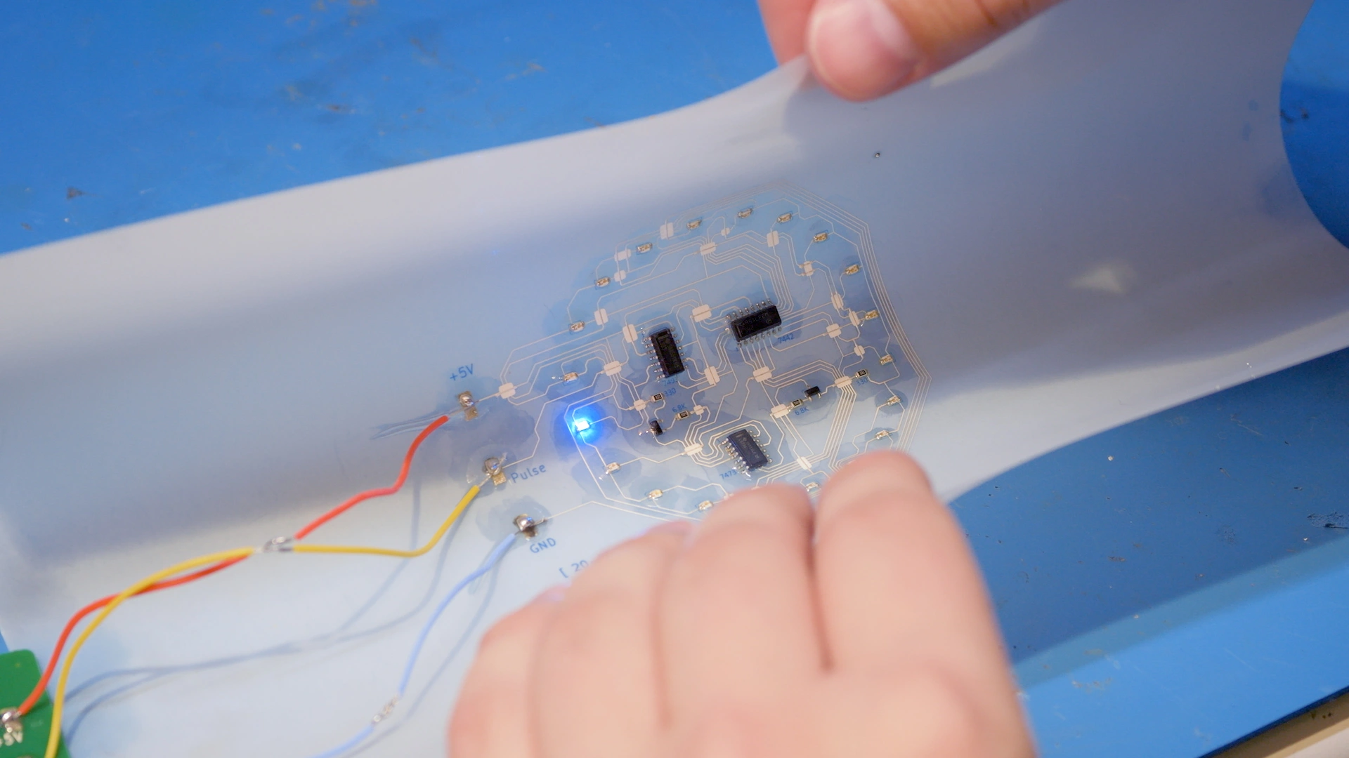
Once connected to an alternating current (140 V, 1.862 kHz), the phosphor layer emits blue light, illuminating the Voltera logo with an even glow across both prints.
Functionality
We determined the Voltera logo would be suitable for this project. It is feasible to incorporate designs into larger electronic applications, including billboards, branded merchandise, and control panels.

Printing the electroluminescent Voltera logo
Base conductive layer
This layer consists of a Voltera logo pattern (55.5 mm L × 19.75 mm W) and positive and negative traces that connect to power and ground terminals.
| Ink | Saral Silver 700 Silver Based Conductive Ink |
| Substrate | Cardstock paper, PET |
| Nozzle type | Nordson EFD 7018424 dispensing tip, 0.15 mm inner diameter |
| Probe pitch | 4 mm |
| Cure time and temperature | 5 minutes at 120°C |


Dielectric layer
This layer features a dielectric Voltera logo pattern which measures 23 mm L × 15 mm W and two dielectric pads. These extra pads help ensure the top conductive layer is appropriately insulated.
| Ink | Saral Dielectric 600 Dielectric Ink |
| Substrate | Cardstock paper, PET |
| Nozzle type | Nordson EFD 7018333 dispensing tip, 0.25 mm inner diameter |
| Probe pitch | 4 mm |
| Cure time and temperature | Air dry for 10-20 minutes |


Phosphor layer
This layer contains a Voltera logo pattern, slightly smaller than the dielectric layer (by 0.5 mm each way), printed with blue light-emitting ink.
| Ink | Saral BluePhosphorL 800 Electroluminescent Ink |
| Substrate | Cardstock paper, PET |
| Nozzle type | Nordson EFD 7018333 dispensing tip, 0.25 mm inner diameter |
| Probe pitch | 4 mm |
| Cure time and temperature | 1 minute at 120°C |


Top conductive layer
Lastly, this layer includes a conductive overlay with an opening at the bottom left to prevent short circuiting. It measures 29.5 mm L × 21.5 mm W and connects to the ground terminal.
| Ink | Saral Conducting Polymer 700 Polymer Electrochromic Ink |
| Substrate | Cardstock paper, PET |
| Nozzle type | Nordson EFD Optimum Chamfered Tip 0.1 mm inner diameter |
| Probe pitch | 1 mm |
| Cure time and temperature | 5 minutes at 120°C |


Challenges and advice for printing multilayer electroluminescent displays
Trapped air
Air bubbles can form in inks that have been left unused for an extended period. These bubbles caused the dielectric layer to break when we cured it in the oven.
Mixing the ink with a dual asymmetric centrifugal mixer before printing will eliminate air bubbles. Additionally, it is recommended to allow the dielectric layer to dry naturally at room temperature instead of curing it in an oven.
Uneven glow
During our experiments, some prints exhibited dark areas, leading to an uneven glow. This issue can arise from several factors:
- The top conductive layer being too thick
- The phosphor layer being too thin or getting scratched off during dispensing of the ink for the top conductive layer
- Irregularities in print height
Adding fiducials to each layer helps improve alignment and print quality. In terms of print settings, if the layer is too thick, increasing the print speed, reducing the height (we reduced it to approximately 40 µm), and using a smaller nozzle can be helpful. If the layer is too thin, try to reduce the print speed.
Furthermore, in multilayer projects, changes in height can happen drastically when printing over existing traces. Setting a low probe pitch will make the height map more accurate, ensuring the height transition at the edges of features is accurate and reducing the risk of traces being printed off-course.
Conclusion

The paper substrate provided consistent results throughout our experimentation, due to its absorbent nature. Each layer was smoother on paper than on PET, highlighting the potential of using paper as a substrate in EL display applications.
On the other hand, PET, being flexible and chemically resistant, offers the advantage of suitability for more demanding use cases. As demonstrated by this project, with careful attention and fine-tuning of the print settings, the results of EL display on PET are equally impressive.
EL displays are also intriguing when printed on glass and other non-conductive substrates. As we continue to explore the possibilities of electroluminescent inks, we invite you to view the other projects we’ve completed.
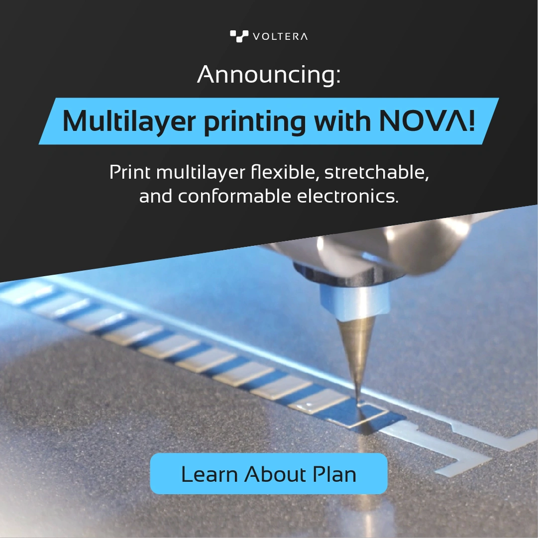
Printing multilayer flexible, stretchable, and conformable electronics?
NOVA’s Plan feature makes it easy.