White paper
Printing a Flexible PCB with Silver Ink on PET
LED applications are popular engineering projects in school. Among these, an LED roulette stands out as it is intellectually challenging and fun. While a roulette circuit is typically printed on a substrate like FR4, printing on a flexible substrate presents further opportunities for education.


- Voltera Conductor 3 silver ink
- ACI Materials FS0142 Semi-Sintering Conductive Ink
- ACI Materials SI3104 Stretchable Printed Insulator
- Voltera T4 solder paste
- Voltera solder wire
- Siraya Tech Tenacious Flexible Resin
- V-One PCB printer
- NOVA materials dispensing system
- Voltera disposable nozzle
- Nordson EFD 7018395 dispensing tip
- Nordson EFD 7018424 dispensing tip
- Nordson general purpose dispense tips
- NE555DR timer
- LEDs
Watch the Video
Project Overview
Purpose
The goal of this project was to prototype a flexible multilayer LED wheel roulette circuit that was traditionally considered rigid and validate the redesign of the circuit.
Design
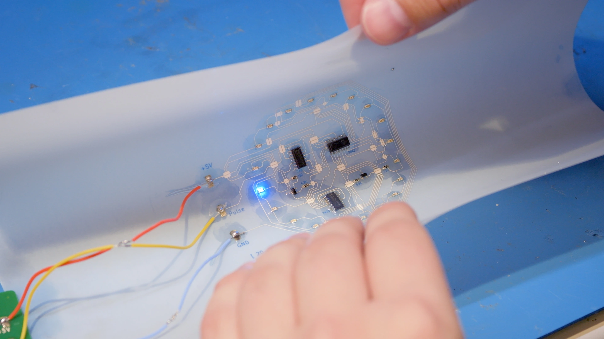
This project involves a multilayer flexible PCB for the LED roulette circuit and a traditional control board that powers it. We adapted the design of an LED roulette circuit, originally developed for a 3” × 4” FR4 board by ITIZ, Voltera’s authorized reseller in Korea. This new version is printed on a coated biaxially oriented PET substrate, allowing the circuit to remain flexible — even when populated with components.


We divided the LED roulette circuit design into three layers:
- Base conductive layer
- Dielectric layer
- Top conductive layer


Desired outcome
We anticipated the circuit would function like a roulette wheel: each time the pulse generator is triggered, the LEDs on the flexible PCB light up in a rapid circular sequence before slowing down and stopping on a single LED.
Functionality
By printing a dielectric and crossover layer on top of the base conductive layer, we created a compact and lightweight LED roulette circuit without using jumpers. Each layer remained flexible after curing, and the circuit maintained its integrity even after encapsulation and repeated flexing.
When connected to power, pressing the switch on the control board caused the LEDs on the flexible PCB to light up, replicating the behavior of a roulette wheel as intended.
Printing the control board
This board controls the pulse signals and powers the LED roulette wheel circuit. We used V-One to print the circuit and reflow the components, which included:
- NE555DR timer
- LED
- Switch
- 47 µF capacitor
- 0.1 µF capacitor
- 10 nF capacitor
- 100 kΩ resistor
- 330 Ω resistor


| Ink | Voltera Conductor 3 silver ink |
| Substrate | 2" x 3" FR1 board |
| Nozzle type | Voltera disposable nozzle |
| Probe pitch | 5 mm |
| Probe time | 4 minutes 38 seconds |
| Print time | 4 minutes 51 seconds |
| Reflow time and temperature | 140°C for 2 minutes, and then 190°C for 30 seconds |


Printing the flexible PCB
This flexible PCB receives signals from the control board and lights up the LEDs as directed.
Base conductive layer
This layer consists of a roulette-shaped circuit (90 mm L × 70 mm W) that connects to the control board, as well as power and ground terminals, with designated gaps for dielectric pads.


| Ink | ACI Materials FS0142 Semi-Sintering Conductive Ink |
| Substrate | PET |
| Nozzle type | Nordson EFD 7018395 dispensing tip, 200 µm inner diameter |
| Probe pitch | 5 mm |
| Probe time | 3 minutes 4 seconds |
| Print time | 14 minutes 42 seconds |
| Cure time and temperature | 150°C for 15 minutes |


Dielectric layer
This layer consists of 29 dielectric pads that provide insulation for the top conductive layer. For better coverage, we printed two passes of dielectric ink.


| Ink | ACI Materials SI3104 Stretchable Printed Insulator |
| Substrate | PET |
| Nozzle type | Nordson EFD 7018424 dispensing tip, 150 µm inner diameter |
| Probe pitch | 5 mm |
| Probe time | 2 minutes 8 seconds |
| Print time | 6 minutes 32 seconds |
| Cure time and temperature | 135°C for 15 minutes |


Top conductive layer
This layer consists of 29 fine crossover traces that connect the paths to the power terminal and control board. To address potential gaps over height changes, we decreased the trace width to 100 mm to enhance trace continuity.


| Ink | ACI Materials FS0142 Semi-Sintering Conductive Ink |
| Substrate | PET |
| Nozzle type | Nordson EFD 7018395 dispensing tip, 200 µm inner diameter |
| Probe pitch | 1 mm |
| Probe time | 2 minutes 46 seconds |
| Print time | 2 minutes 26 seconds |
| Cure time and temperature | 150°C for 15 minutes |


Post-processing the flexible PCB
Dispensing solder paste and reflowing the components
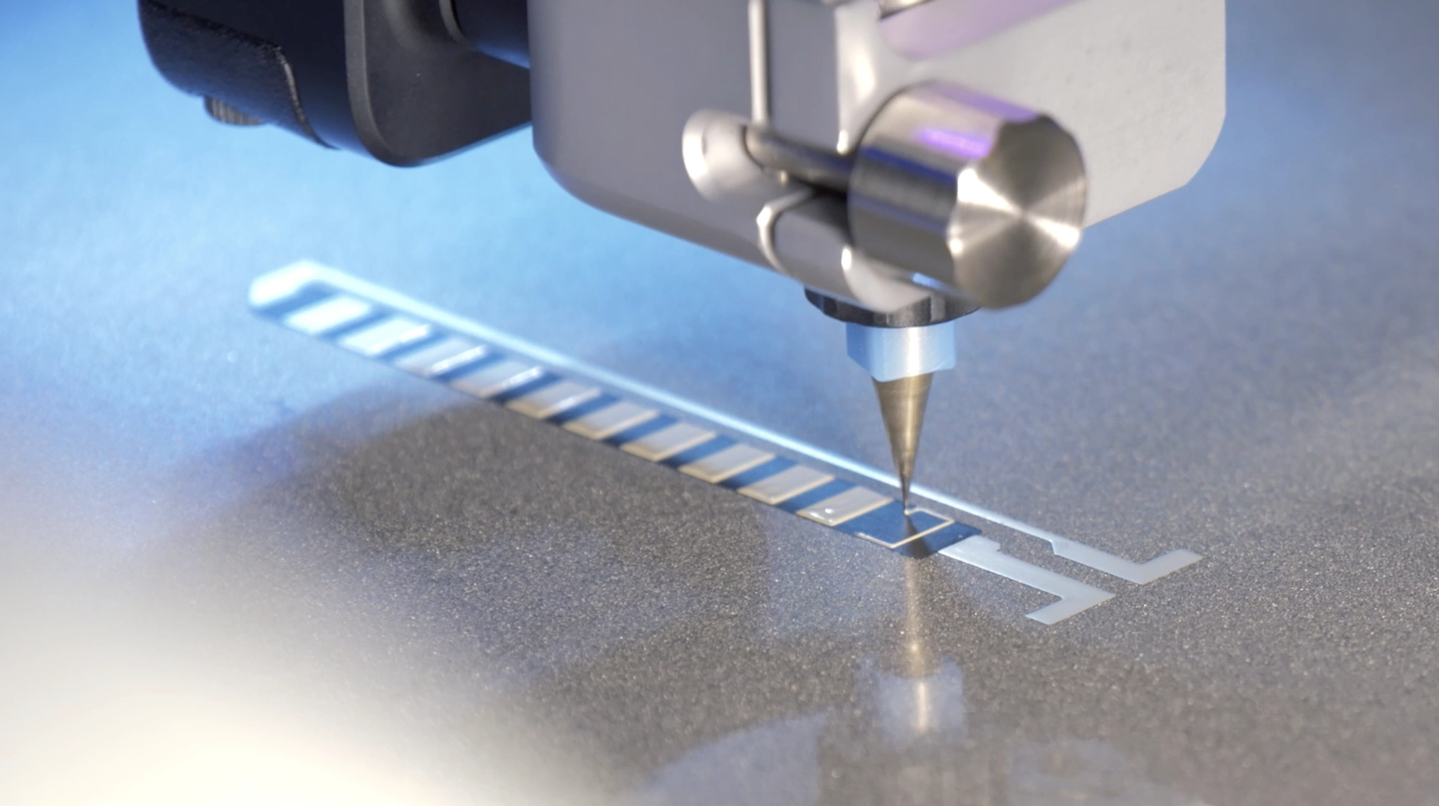
Once the circuit was cured, we dispensed solder paste using NOVA and populated the components before reflowing them in an oven.
| Ink | Voltera T4 solder paste |
| Substrate | PET |
| Nozzle type | Nordson general purpose dispense tip, 410 µm inner diameter, blue |
| Probe time | 2 minutes 6 seconds |
| Print time | 4 minutes 39 seconds |
| Cure time and temperature | 150°C for 2 minutes |


Because the wires are not heat-resistant, we manually soldered them onto both the companion board and the flexible roulette circuit.
Encapsulating the components
To reinforce their connection to the substrate, we dispensed encapsulation resin using a syringe onto the components and cured the resin in a UV light box.
| Ink | Siraya Tech Tenacious Flexible Resin |
| Substrate | PET |
| Nozzle type | Nordson general purpose dispense tip, 330 µm inner diameter, orange |
| Cure time and temperature | Room temperature for 2 minutes under UV light |


Once cured, we manually soldered the wires of the control board and the wires of the flexible roulette circuit together.


Challenges and advice
Electrical shorts
We encountered issues with shorts due to multiple crossover lines on the dielectric layer. To address this, we recommend printing a second pass of the dielectric layer to achieve a thicker insulating layer that better supports additional layers printed on top.
Drastic height changes
A second pass of the dielectric layer can result in significant height differences. To handle this, it is advisable to set a low probe pitch to ensure a more accurate height map and print a thicker crossover layer for improved contact on the top layer.
Maintaining flexibility with components attached
To ensure the circuit remained flexible after populating components, we opted for smaller, more flexible components. This, combined with the use of a flexible substrate, encapsulant, and inks, allowed the circuit to bend without damaging the connections.
Conclusion
This project highlights the educational value of converting rigid circuit designs into flexible ones, allowing students to explore diverse materials and optimize print settings through experimentation. It also demonstrates the potential of prototyping flexible PCBs to replace electronics that were considered rigid, achieving lightweight, compact, and resilient designs.
As flexible PCBs gain more popularity, hands-on experience with these technologies becomes essential for staying ahead in the rapidly evolving electronics industry. We invite you to explore our other projects as we continue to explore the possibilities of flexible PCBs and printed electronics.

Printing multilayer flexible, stretchable, and conformable electronics?
NOVA’s Plan feature makes it easy.

