Autodesk ❤ Voltera
EAGLE now has Voltera design blocks for even faster prototyping!
They’ll be live in Version 8.3.4 but you can get them right now from their site.

What are design blocks?
After their acquisition by Autodesk in 2016, the great folks at EAGLE got to work on plenty of new features to make PCB design easier and faster.
One of these new features is modular design blocks. These design blocks allow you to design common key features or circuit modules once and then use them in multiple designs. Now, while this is great for folks with designs that have repeated features, it is also fantastic news for all Voltera V-One users.

Making a PCB using an Arduino design block
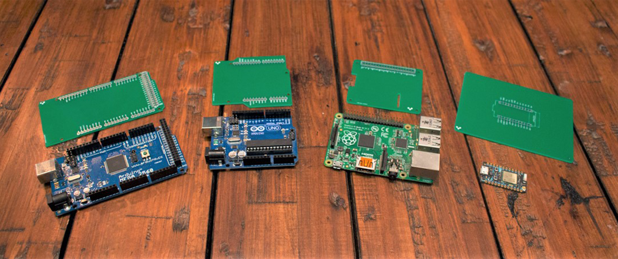
All our standard substrates have registration markings to align your digital design to the physical board. With the new design blocks, you will automatically be given the board as a schematic part and layout part. Let’s see it in action!
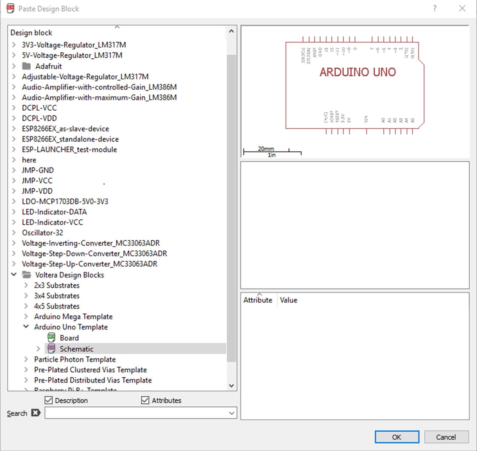

Step 1: Open EAGLE and select a design block
As previously mentioned, the blocks will be live in version 8.3.4 but can be downloaded from here until then. In this example we’re using the Arduino Uno template.
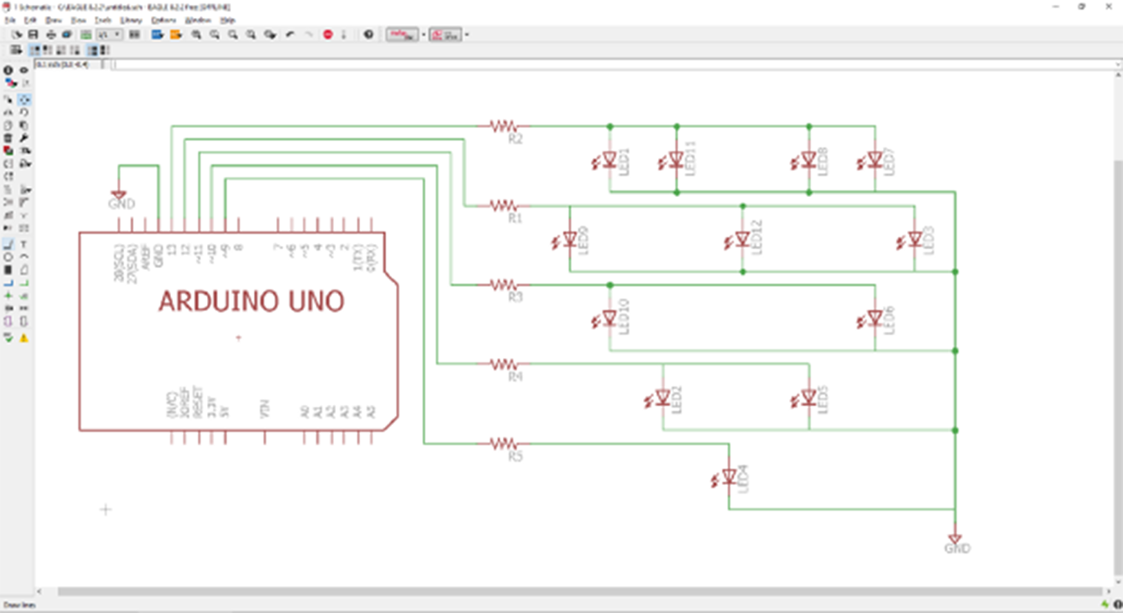

Step 2: Design your schematic
The design block automatically creates the component drawing for the Uno.
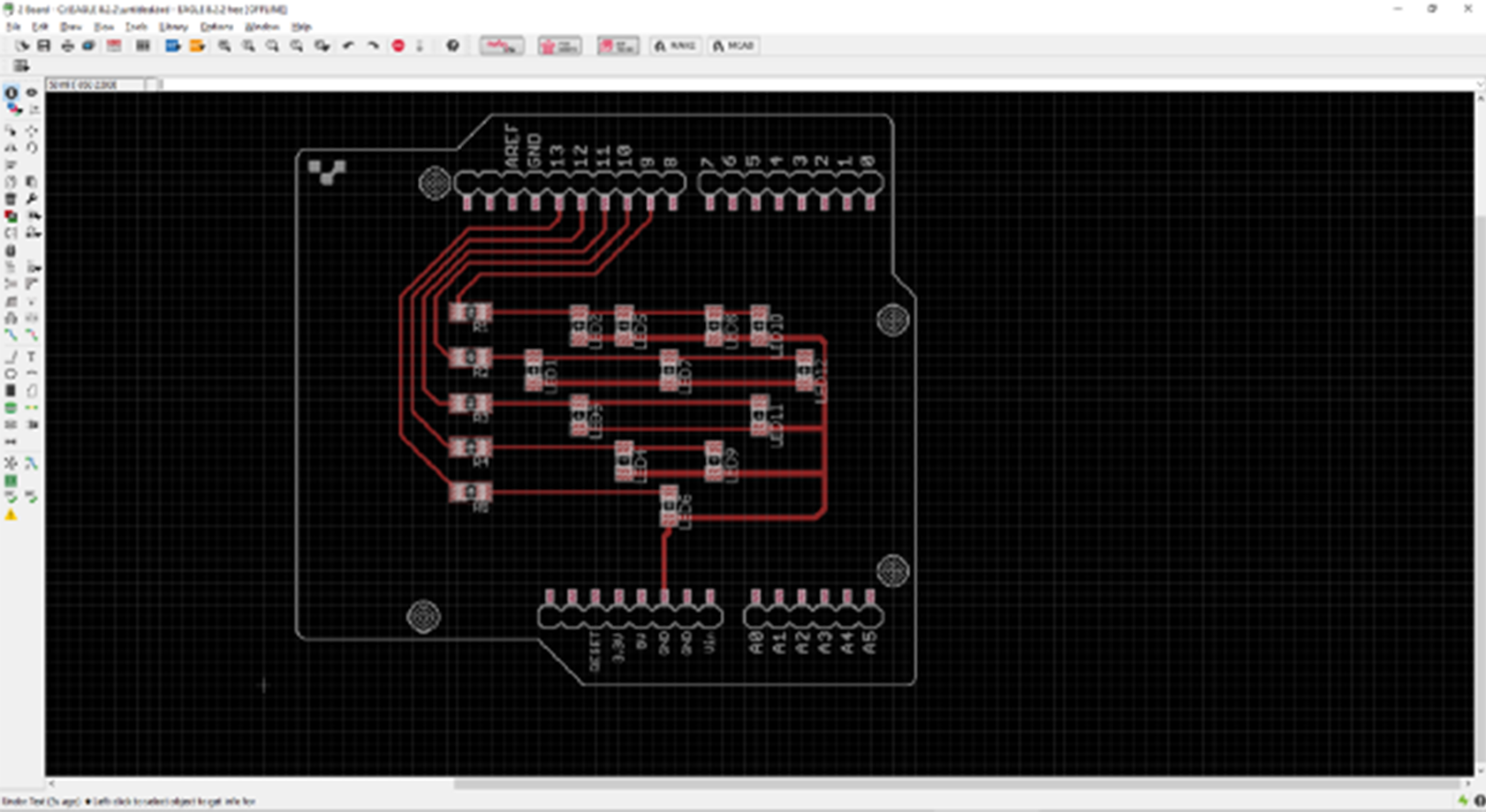

Step 3: Design your layout
The design block also automatically creates the board outline, mounting locations, and pinouts for the Uno Template board.
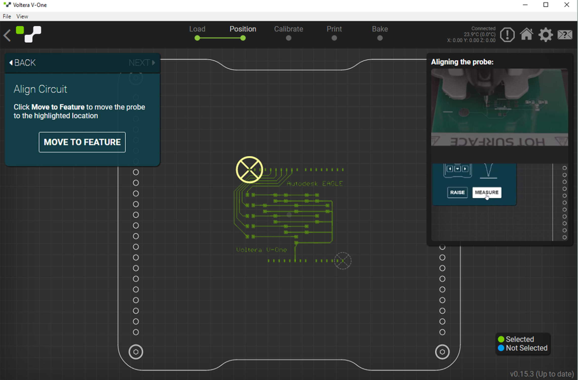

Step 4: Export to Gerber, import to Voltera software, and align digital features to physical features
The printer software knows what your design looks like but needs to be told how to line it up with the pads and holes that are already on the physical Uno template. As you can see above, the software guides you through a simple alignment process within a couple minutes.


Step 5: Print and thermally cure circuit
Printing took about 5 minutes and curing took about 20. That was more than enough time to program the Arduino code to flash the LEDs we’re using.
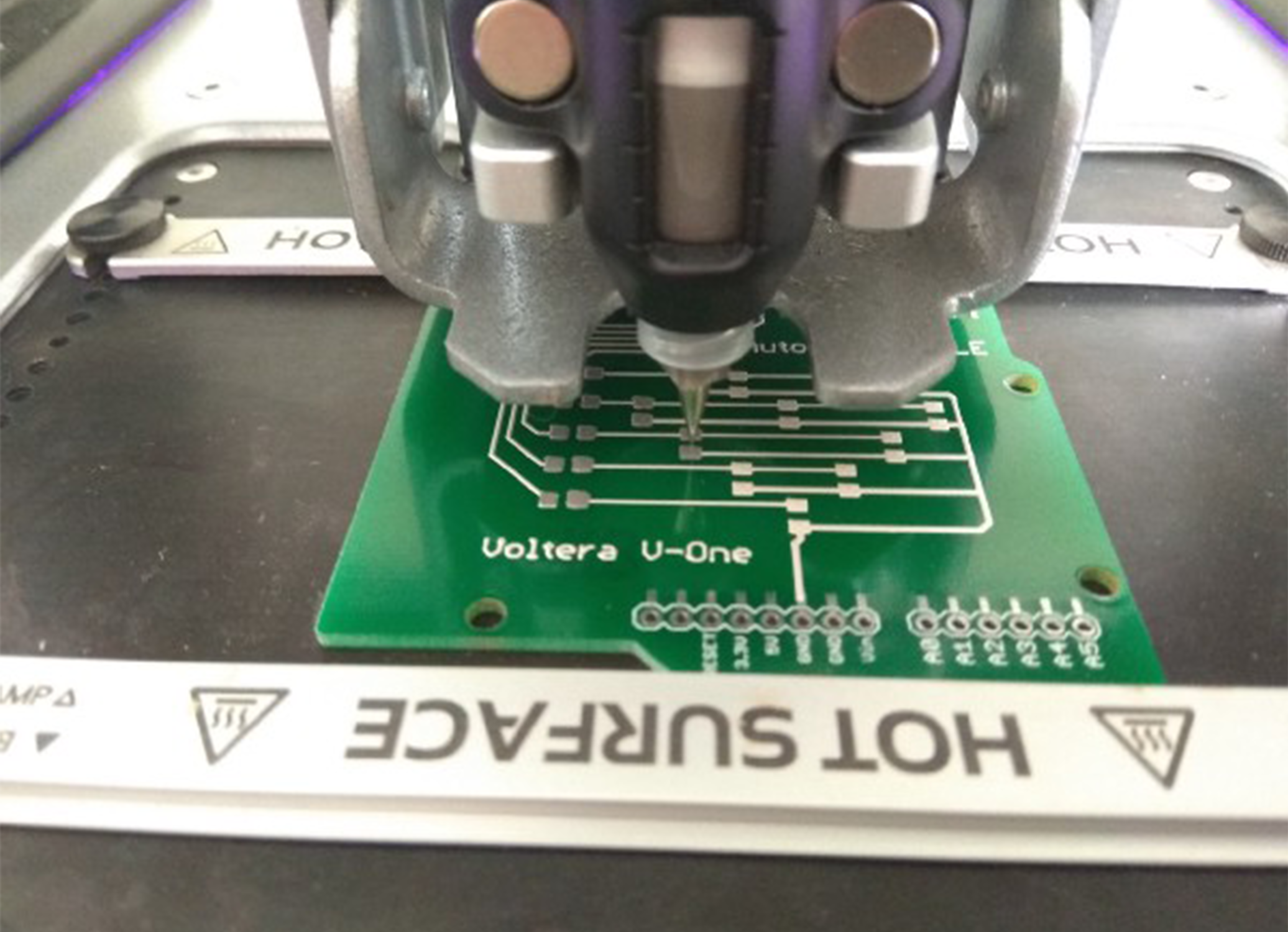

Step 6: Dispense solder paste, mount components, and reflow
Since the Voltera software already had the Gerber files, it was also able to dispense the solder paste in a couple minutes.
It took another couple minutes to add the components and then get a coffee refill while the board reflows.
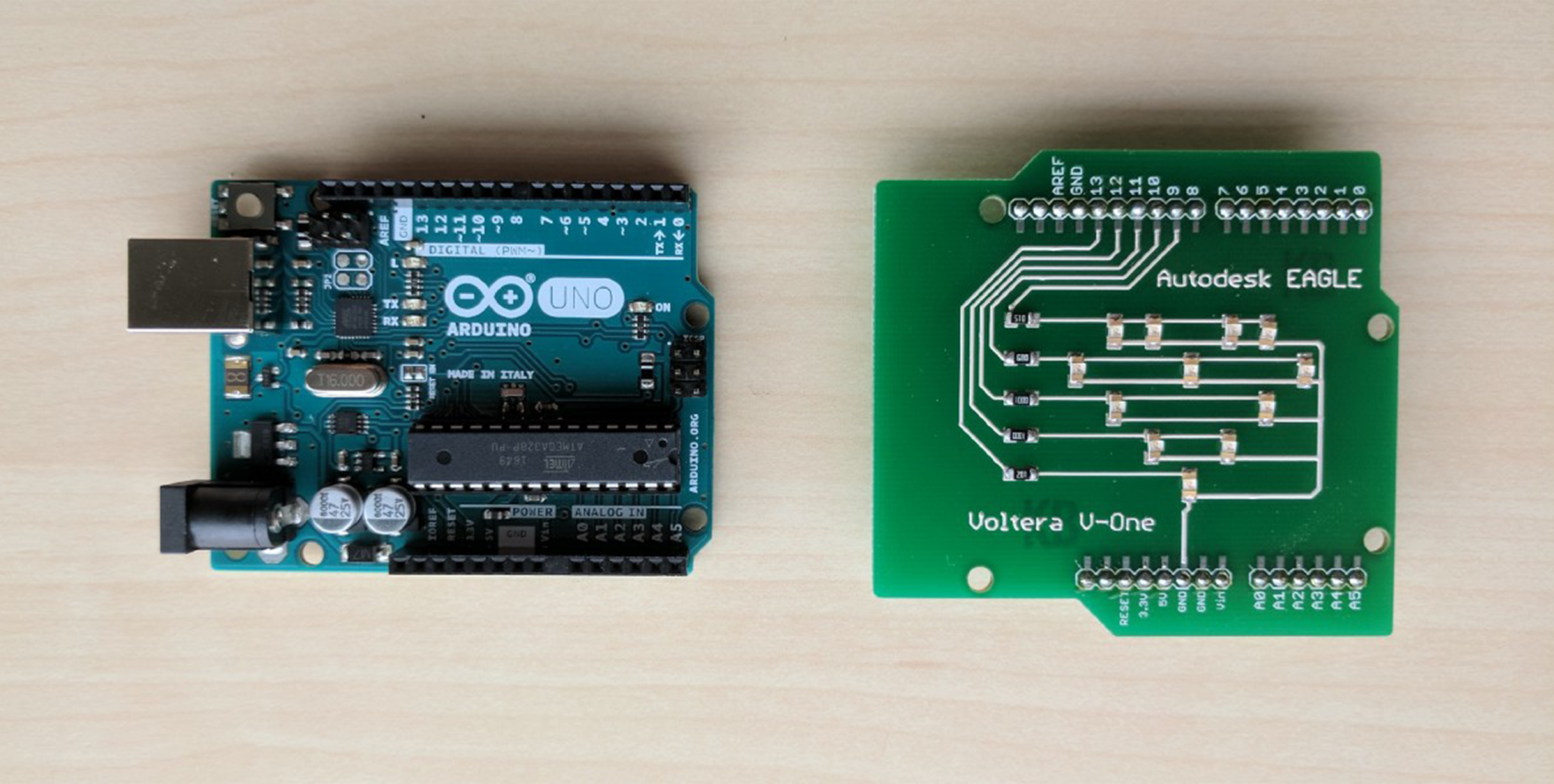

Step 7: Mount your new shield
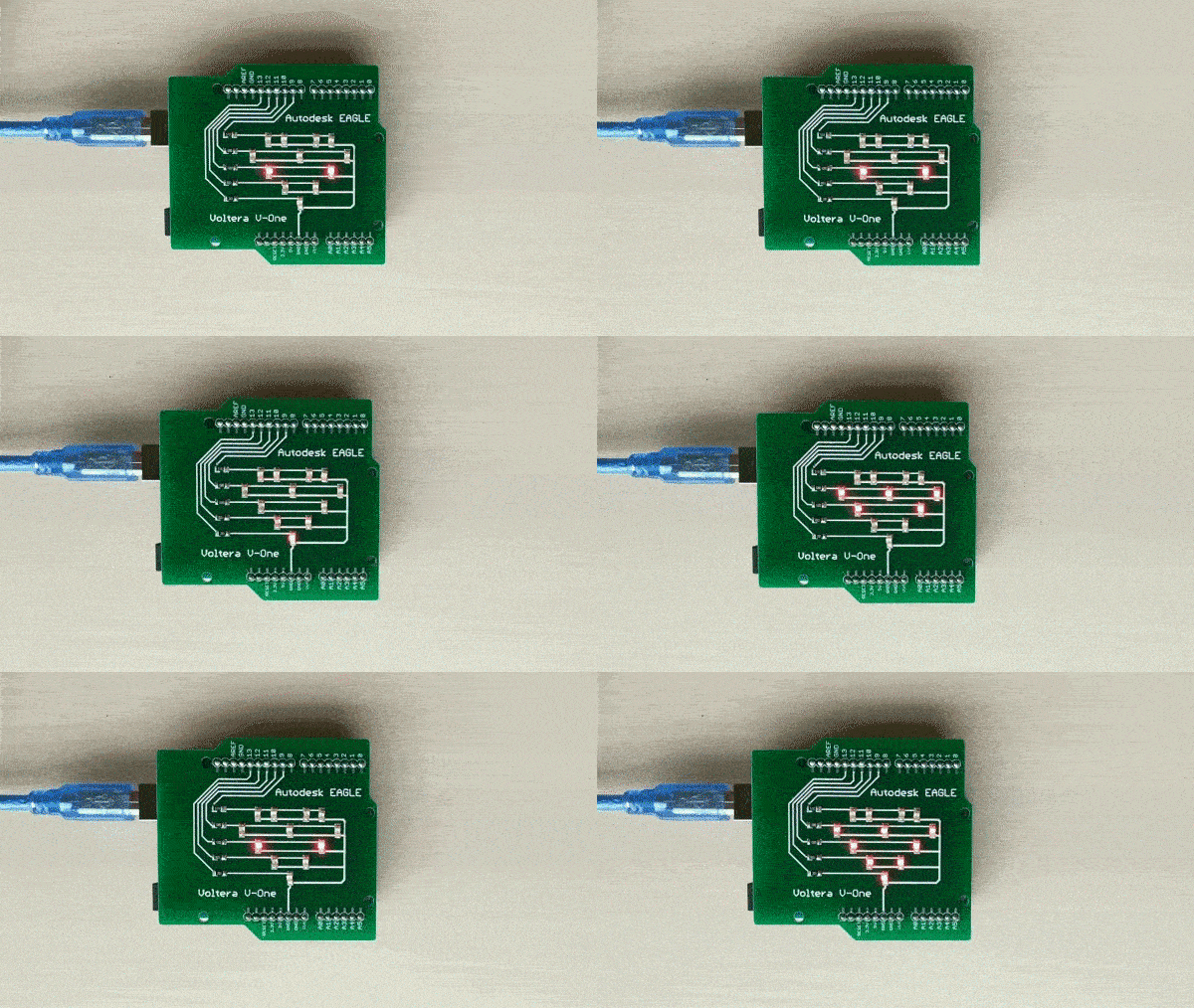
All in all, this entire project took us less than 2.5 hours to design, purchase components, print, cure, program, populate, and reflow. About a third of that was curing and reflowing which are completely hands-off steps.
Designing the circuit definitely was the most intensive part and this was obviously a simple circuit. It would have taken even more time but the design blocks relieved a lot of the load there.


We’re pumped to soon be supported out-of-the-box in EAGLE. Until then, grab the design blocks and a template board to get started.
Interested in learning more about PCB design? Check out these resources:
Check out our Customer Stories
Take a closer look at what our customers are doing in the industry.
