Fully 3D-Printed Carbon Nanotube Field Emission Electron Sources with In-Plane Gate Electrode
Field emission has a long history; it has been studied by researchers since the 1880’s. Propelling many breakthroughs in our fundamental understanding of physics, field emission gave quantum mechanics an early triumph in the 1920’s through the phenomenon of quantum tunneling, and led to the invention of the Field Electron Microscope in 1937 so researchers could peer more deeply into the mysteries of nature than ever before.
Today, the most compelling breakthroughs in the science of field emission come from the manufacturing techniques used to create the emitters, and the incredible applications these techniques could enable in our technological world.
In this post we’ll be looking at a collaboration between Imperio Anel Perales-Martinez of the Escuela de Ingenieria y Ciencias, Tecnologico de Monterrey, and Luis Fernando Velasquez-Garcia of the Microsystems Technology Laboratories at the Massachusetts Institute of Technology (MIT). Together, they created the world’s first fully additively manufactured carbon nanotube field-emission electron source, developed with direct ink writing (DIW), one of the least expensive and most versatile manufacturing methods available. Their technology could be used to miniaturize mass spectrometry, create hand-held X-Ray devices, or even allow for the electric propulsion of nanosatellites.
What is field emission?
Field emission is a technique for creating a beam of electrons with an electric field. Being tiny, subatomic particles, electrons exhibit exotic quantum properties under certain conditions. One of these properties is called quantum tunneling, a phenomenon where electrons can pass through barriers based on the thickness of the barrier and the energy of the electron. This occurs because electrons can behave like both a particle and a wave, one of the counterintuitive aspects of quantum mechanics that inspired Einstein to describe the field as “spooky” (tongue firmly in cheek).
Imagine a basketball bouncing against a metal wall. The basketball itself will rebound, but the sound of the collision can be heard from the other side: the basketball itself behaves like a particle, but the sound is a wave that passes through the barrier. How much of the sound passes through depends on how thick the wall is, or how hard you hurl the ball. Unlike basketballs, electrons can behave as both a particle and a wave, so when you hurl a lot of them at a wall, some tunnel through (behaving like waves) while many more are reflected (behaving like particles). This is how scientists create the beam.
Field emitters work by tuning both the thickness of the wall (the strength of the electric field) and the power of the throw (the bias voltage between the emitting electrode and the extractor gate) to precisely pull a thin stream of electrons through a barrier in a controlled manner.
The last ingredient is a fine tip. The earliest Field Electron Microscope, invented by Erwin W. Mueller, used a sharpened wire in a vacuum surrounded by phosphor screen for image detection: a rudimentary instrument (if impressive for the time). The tip of the wire was sharpened because the emission electrode, the thing that fires the electrons at the extractor gate, has to be the right shape to spark the quantum tunnelling process that generates the thin electron beam. Modern field emitters favor more sophisticated materials, like the carbon nanotube ink (CNT) used for the device created in this paper. CNTs are highly conductive -- allow electrons to move through them easily -- and have an ultra fine tip by definition (as nanotubes).
This beam of electrons can then be used in a variety of ways: to make measurements (like in a scanning electron microscope, by bouncing the stream off a sample and measuring how they scatter to form an image) or help propel a vehicle (like keeping charge neutrality in a nanosatellite that uses electric rockets to navigate through the vacuum of space).
Why 3D printing (direct-ink-writing additive manufacturing)?
One of the most notable aspects of the collaboration between Perales-Martinez and Velasquez-Garcia is that their field emitter is entirely additively manufactured using direct-ink writing (DIW): they 3D printed the device. This is a valuable development for a number of reasons:
Accessibility and affordability
DIW is one of the cheapest methods available for an application such as this. With DIW, you deposit materials only where you need them, reducing waste (and helping the environment). You also don’t need to pay for expensive subtractive processing or equipment: for a modest, one-time investment in a direct-write printer, you can deposit various circuit designs on numerous substrates without worrying about minimum order quantities, overseas shipping costs, or long lead times. Most importantly, you don’t need any tools or masks to create your patterns; you simply load a design file into the printer’s software and deposit it onto your substrate. As is the case with all 3D printing techniques, the on-demand production of personalized goods -- making what you need when you need it -- offers more sustainable freedom to iterate on designs.
Materials freedom
With a DIW 3D printer designed to deposit various viscous, thixotropic materials on any substrate, you can make design changes quickly and easily, and even switch printing materials on the fly precisely aligning the layers without needing to swap out a frame, mold or die. You can simply make a change in your circuit design software, reupload your file, and create the new pattern instantly. This enables the production of exotic circuit designs, like electronics printed on flexible and stretchable substrates, or electronics printed directly onto a device enclosure. For example, in aerospace applications with extreme weight constraints, the ability to print a field emitter for propulsion directly on to the nanosatellite enclosure without adding the weight of a substrate is attractive.
Development speed
DIW saves valuable time. Given both of the above, it’s clear that DIW techniques allow for faster iteration than traditional tooling-based approaches. Having a tool on your benchtop that fabricates circuits allows for much quicker design iteration than any other available technique. It also allows researchers and designers to keep their intellectual property completely in-house.
By using DIW techniques, Perales-Martinez and Velasquez-Garcia were able to manufacture CNT field emission sources at $2.50 per device, lower than screen printing and significantly less than cleanroom manufacturing.
How to print a field emitter
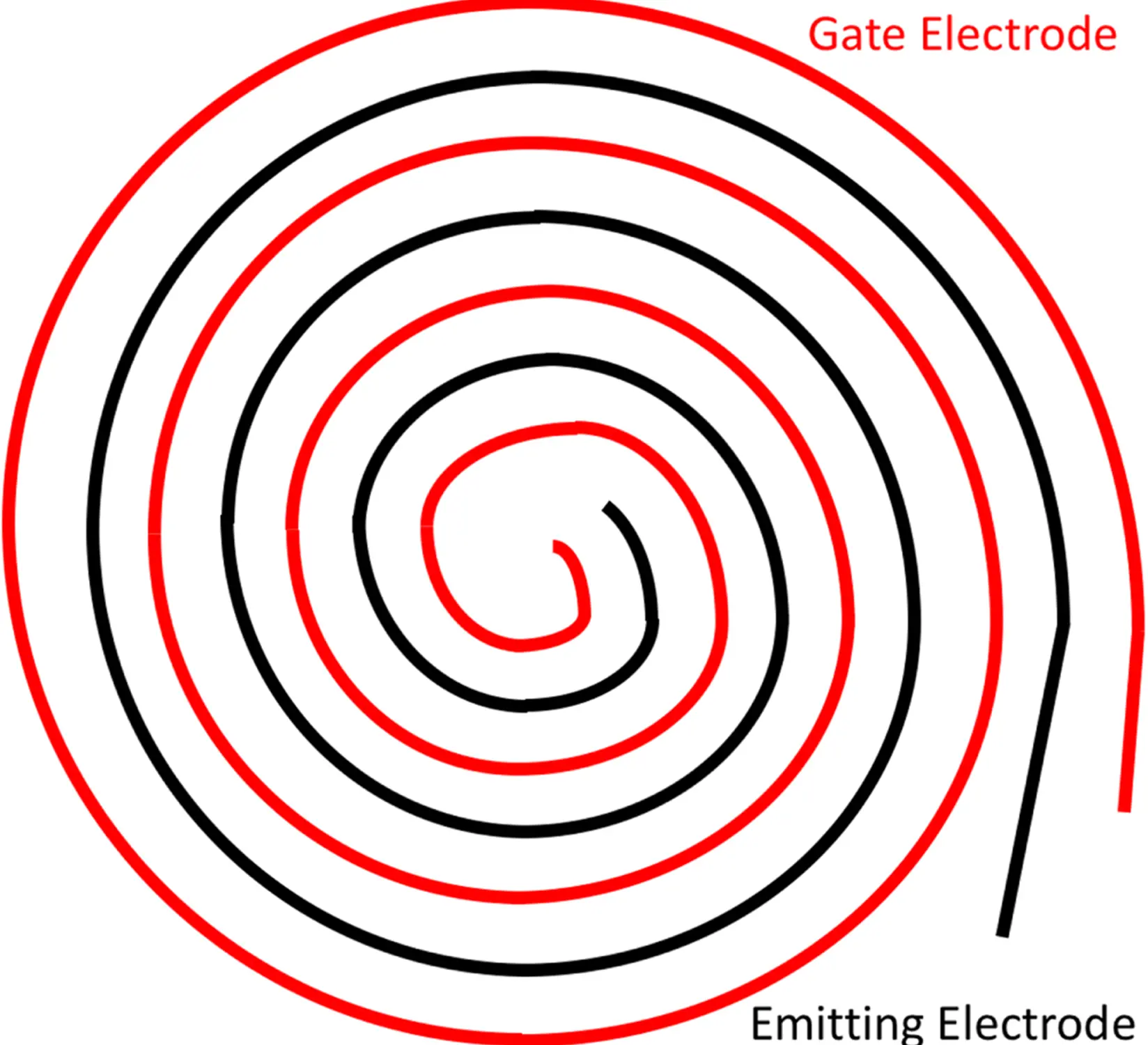
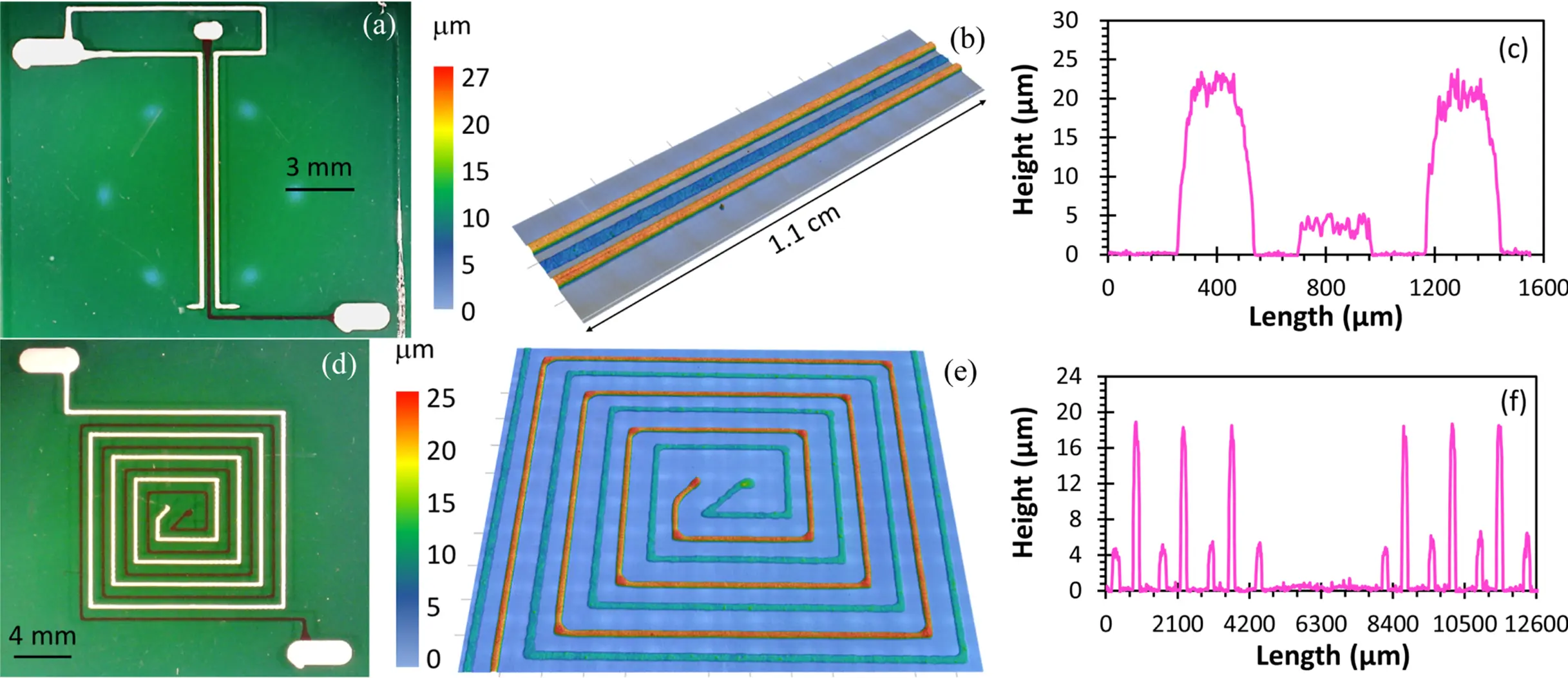
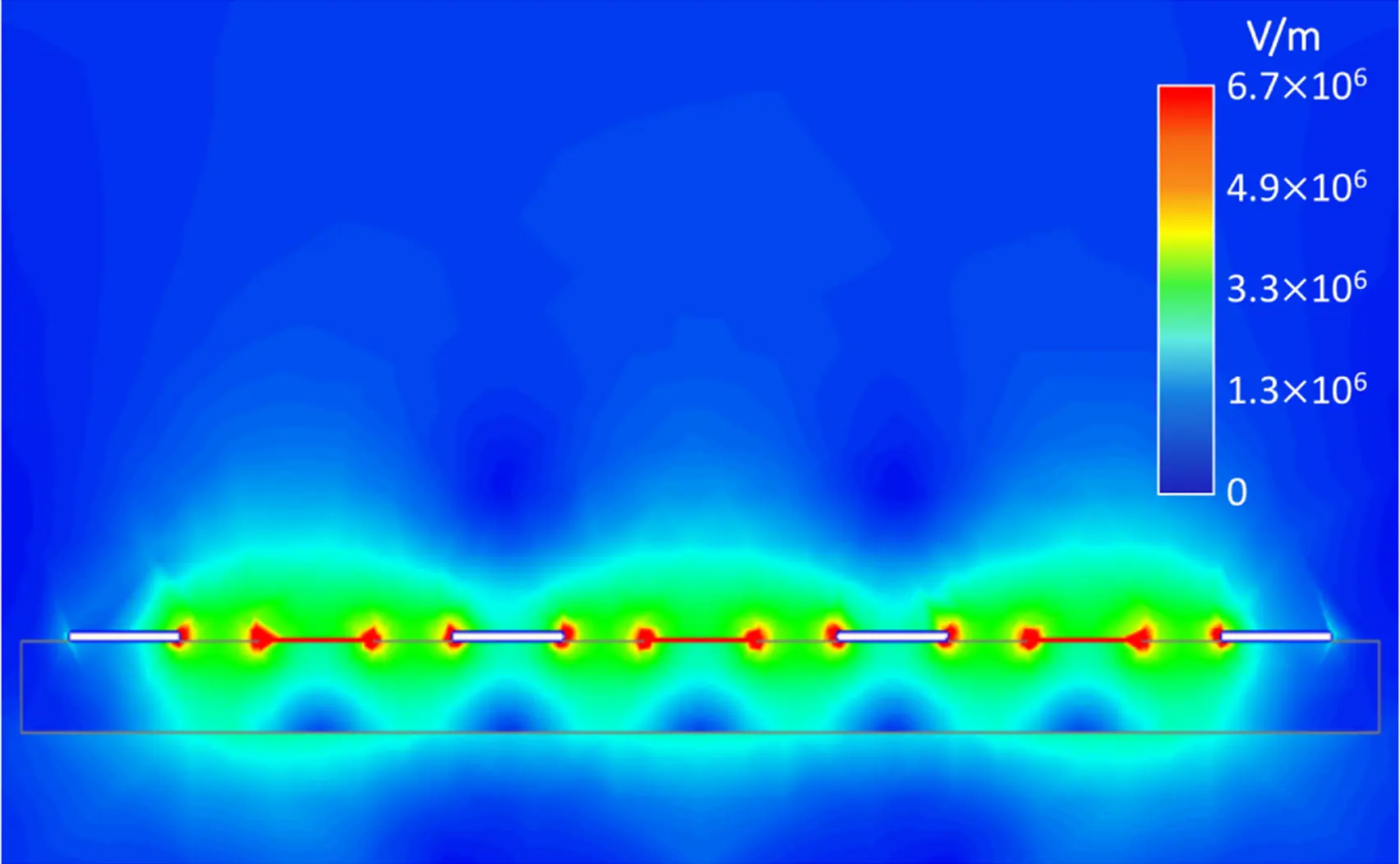
Perales-Martinez and Velasquez-Garcia made two cases of field emitters: a 25mm straight trace of CNT, and a 135mm square-loop spiral with 0.5mm gap. Their devices were 2.5cm square glass substrates coated with a trace of CNT ink as an emission electrode, and silver (Ag) microparticle ink as the in-plane extractor gate.
The silver microparticle ink was Voltera’s conductive ink, the CNT ink was a custom formulation: carboxylic acid-functionalized multiwalled CNT’s (N, N dimethylformamide, ethyl cellulose).
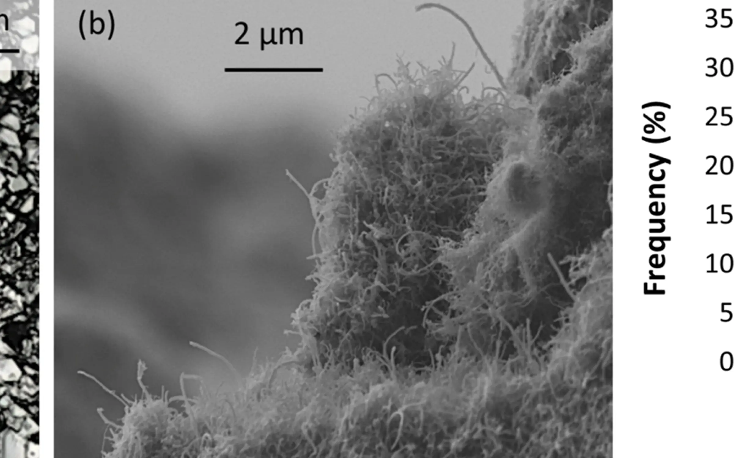
They tested these devices in several ways. First, they performed a thermogravimetrical (TGM) analysis of the CNT ink to measure its mass during burn-off, to make sure annealing temperature caused the filler of the ink (ethyl cellulose) be removed without damaging the CNTs. Then, they performed rheology tests of the inks with a rheometer, and tested the surface structure of the inks with an SEM. Next, they tested the electrical resistivity with a sputtered-silver glass chip to verify the ink was conductive enough for their application. Finally, the field emitters were tested in vacuum, with up to 850V bias between the silver and CNT imprints, and a 1300V floating external electrode. In all, these desktop-printed devices were impressive, comparing well with other devices in literature which were made in semiconductor cleanrooms.

Given the robust performance of these field emitters, and the potential applications lent by their inexpensive, lightweight and compact nature, Perales-Martinez and Velasquez-Garcia results are extremely exciting – and precisely the kind of research that we at Voltera love to see conducted with our tools.
Stay tuned for a future post where we sit down with Luis Fernando Velasquez-Garcia of MIT to discuss his work, his experience using the V-One PCB printer, and how future products from Voltera might allow for even more powerful breakthroughs in the future.
Check out our Customer Stories
Take a closer look at what our customers are doing in the industry.