Screen Printing vs. Direct Ink Writing for Printed Electronics
In the ever-evolving landscape of advanced manufacturing and material deposition, screen printing and direct ink writing (DIW) have emerged as two prominent technologies. Both techniques have found applications across various industries, including display electronics, biomedical devices, and energy storage systems.
Understanding the differences between these two methods is crucial for selecting the appropriate technology for specific applications. This blog will explore the key differences, advantages, and limitations of screen printing and DIW.
Screen printing
Screen printing is a well-established technique widely used in the field of printed electronics. It involves the use of a mesh screen to transfer conductive inks, dielectric pastes, or other functional materials onto a substrate, except in areas made impermeable by a blocking stencil. The ability to print a variety of materials, such as silver, carbon, and dielectric inks, makes screen printing essential for flexible and rigid electronics.
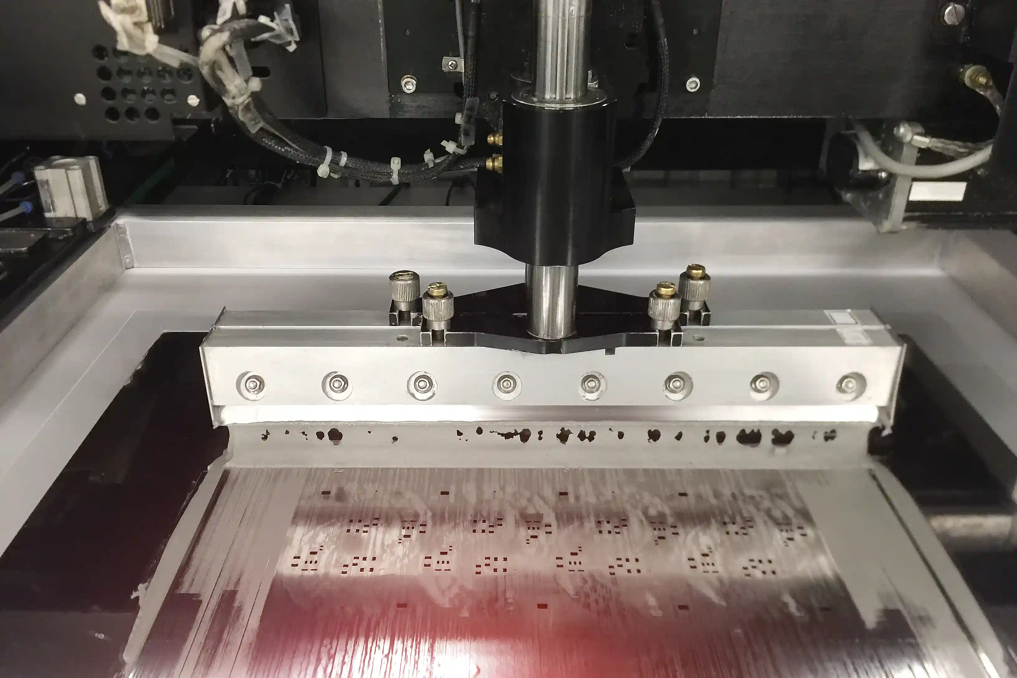

How screen printing works
The screen printing process in printed electronics involves several key steps:
- Screen preparation: A mesh screen is coated with a photosensitive emulsion and a stencil of the desired circuit pattern is created by exposing the emulsion to light through a film positive. The unexposed areas of the emulsion are washed away, leaving a stencil that defines the electronic pattern on the screen.
- Ink application: Conductive or functional ink is placed on the screen, and a squeegee is used to press the ink through the mesh openings, transferring the pattern onto substrates such as PET, polyimide, or other materials commonly used in electronics.
- Curing: The printed substrate is typically cured using heat, UV light, or other methods to solidify the ink and ensure proper conductivity and adhesion.
Advantages of screen printing in printed electronics
- Scalability: Screen printing is ideal for large-scale production of printed electronics, such as RFID antennas, flexible circuits, and wearable sensors, offering a cost-effective solution for mass manufacturing.
- Versatility: Screen printing supports a wide range of conductive, resistive, and insulating materials, allowing for the fabrication of diverse electronic components on various substrates, including flexible and rigid surfaces.
- Thick film deposition: Screen printing excels in depositing relatively thick layers of conductive or dielectric inks, which is advantageous in applications like thick-film resistors and printed circuit boards where material build-up is essential for functionality.
Limitations of screen printing
- Costs: Initial setup costs, including screen preparation and stencil creation, can be high, especially for small runs or frequent design changes. Specialized inks are also costly, and material waste, particularly of expensive inks, adds significantly to the overall expense.
- Resolution: The resolution of screen printing is constrained by the mesh size, limiting the minimum achievable line widths and spacing. This makes it challenging for applications requiring fine feature sizes, such as advanced microelectronics.
- Complexity in multilayer printing: While screen printing is capable of creating multilayer structures, aligning each layer accurately is critical and can be complex. Misalignments can lead to electrical short circuits or open connections, impacting the performance of printed electronic devices.
Direct ink writing
DIW is an additive manufacturing process that deposits conductive inks, solder pastes, and other functional materials onto substrates, layer by layer. Similar to screen printing, DIW technology is compatible with a wide variety of materials, but unlike screen printing, which prints entire patterns at once, DIW creates patterns feature-by-feature. This allows DIW machines like NOVA to offer precise control of the material dispensed and makes it ideal for prototyping and customization of printed electronics.
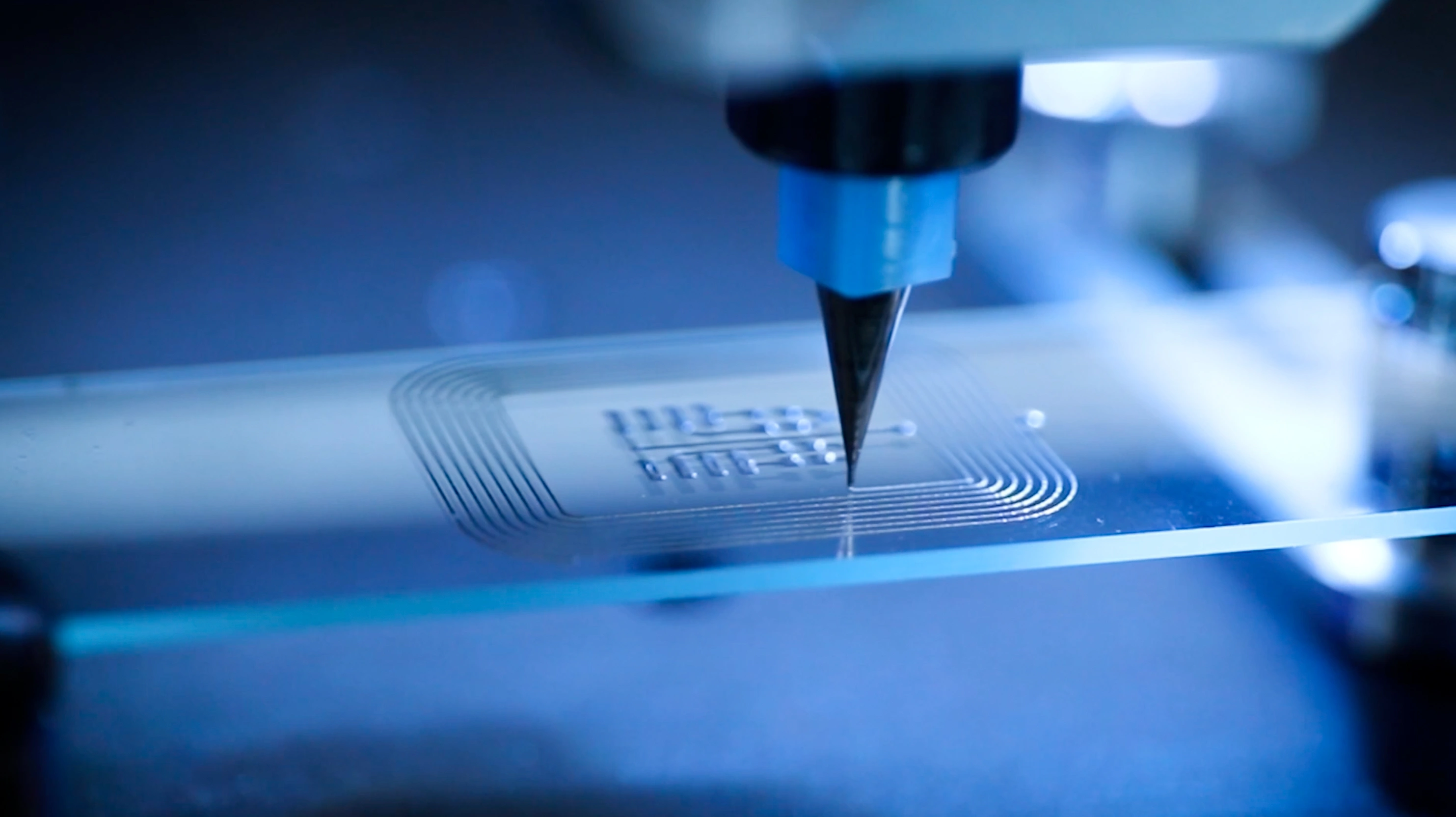

How direct ink writing works
The DIW process in printed electronics involves the following steps:
- Ink/paste preparation: Depending on the material, inks or pastes may need purging to remove trapped air. For solder pastes, it's crucial to let the cartridge reach room temperature before dispensing.
- Dispensing: The ink is extruded through a nozzle, following precise paths controlled by software. The nozzle moves relative to the substrate, dispensing material onto specific areas to create intricate electronic patterns layer by layer.
- Curing: The dispensed material is typically solidified through heat or UV light, ensuring the conductivity and stability required for electronics to function.
Advantages of direct ink writing in printed electronics
- High precision: DIW offers high resolution, allowing for the creation of fine, detailed features that are ideal for intricate electronic patterns and components. This precision makes it suitable for applications requiring meticulous design and control over material placement.
- Material versatility: DIW printing supports a variety of materials, including conductive inks, composites, epoxies, encapsulants, and multi-materials, enabling complex and functional electronic structures.
- Customization: DIW is perfect for prototyping and small-batch production, offering flexibility and easy design adjustments, ideal for custom electronic applications.
- Scalability to screen printing: DIW is highly compatible with screen-printable inks or pastes, making it easy to transition from prototyping with DIW to large-scale deployment with screen printing.
Limitations of direct ink writing in printed electronics
- Speed: Although the setup process is simpler, DIW builds patterns feature by feature, making it slower compared to the rapid, full-pattern deposition of screen printing.
- Material preparation: DIW relies on ink cartridges, which may run out during the printing process, requiring frequent reloading and causing downtime for material changeovers. This can interrupt the workflow.
- Scale: Due to the workflow of DIW, scaling up to mass production is challenging compared to screen printing.
Screen printing vs. DIW: When to choose which?
The choice between screen printing and DIW in printed electronics depends on the specific needs of your application. Screen printing is well-suited for high-volume production where speed and cost-efficiency of manufacturing are crucial. As such, it’s ideal for large-scale manufacturing of electronics.

On the other hand, DIW is the preferred choice for applications that require high precision, customization, and the ability to work with advanced materials. Applications such as biomedical devices and microelectronics can benefit from DIW due to its ability to create complex geometries and functional structures, especially during the prototyping stage when frequent design changes are common.
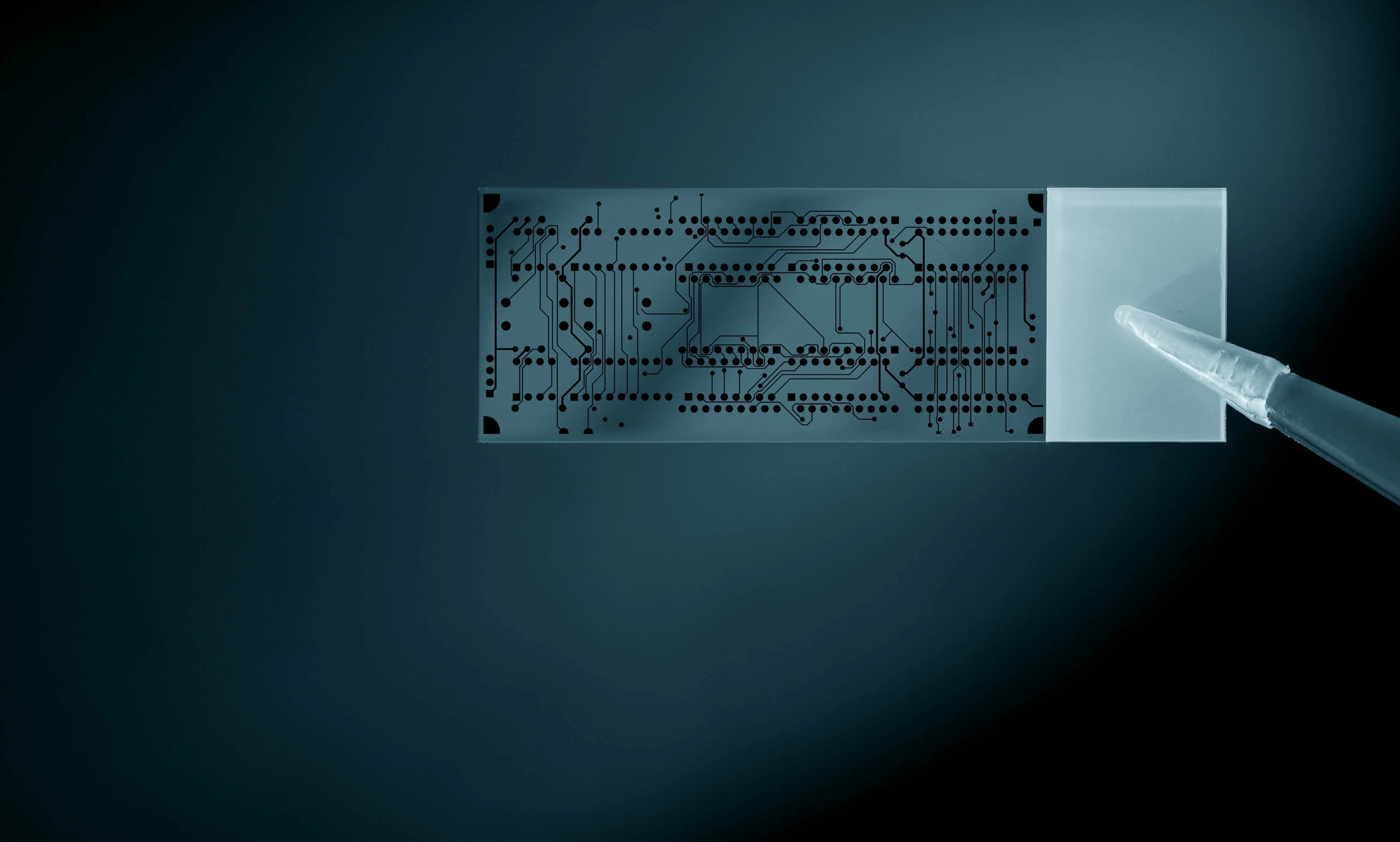

Using the NOVA materials dispensing system as an example, here’s how it stacks up against screen printing:
| Criteria | NOVA | Screen printing |
|---|---|---|
| Tooling requiredequired | No tooling required | Requires custom stencils or screens for each design, significantly increasing costs for small batches |
| Rapid iteration | Yes. Users can test a material or create a prototype in less than an hour. | No. Time-consuming and costly stencil changes are required. |
| Material waste | Precise control over material deposition, minimizing waste | High material waste due to excess ink usage and stencil cleaning |
| Ease of use | Easy to use, with intuitive software | Requires experience and manual setup |
| Accessibility | Accessible to both novices and experts | Requires intensive training to get started |
| Trace width | A minimum trace width of 0.1 mm, with no added cost, providing high precision and allowing for the creation of fine, detailed features | Trace widths narrower than 5 mils (0.127 mm) will increase the cost significantly |
| Layer count | 4 stackup layers; multiple materials can be assigned to each layer | Typically limited to 2 layers, more layers require complex setup |
| Compatible materials | About the same as screen printing. It supports most screen-printable materials, including conductive inks, composites, epoxies, encapsulants, and custom inks. | Supports a wide range of inks, pastes, and adhesives |
| Alignment accuracy | Camera assisted alignment, with a 17 µm/px camera resolution, about the same as screen printing | Manual or semi-automatic alignment, accuracy varies |
| Print thickness | About the same as screen printing and dependant on ink viscosity | 10 - 20 µm per layer |
Conclusion
Deciding between screen printing and DIW comes down to what your project needs most. Knowing the strengths and limitations of each method helps you match the right technology to your design goals, whether you're focusing on scalability, precision, or working with advanced materials in printed electronics.
For more information on technologies in printed electronics, check out the following blogs:
- Introduction to Direct Ink Writing (DIW) Printing Technology
- Introduction to Screen Printing
- Introduction to Inkjet Technology
- Introduction to Gravure Printing Technology
Meanwhile, if you have questions about your PCB printing needs, please contact us at sales@voltera.io or book a meeting with us!
References
Check out our Customer Stories
Take a closer look at what our customers are doing in the industry.
