There's No Such Thing as a Printed Electronics Engineer
I know what you must be thinking — “Hey Alroy, I know plenty of electronics engineers, and PCB stands for printed circuit board. Is printed electronics different? What are you talking about?”


My point exactly.
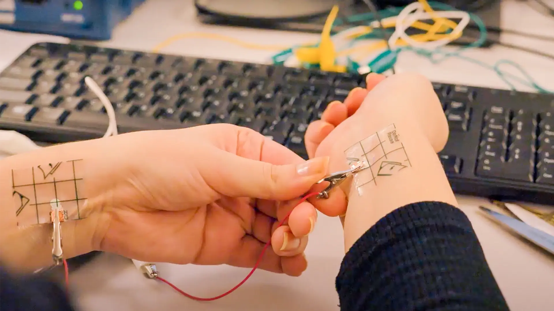
Printed Electronics (PE) refers to using conductive inks to create circuits that need to be flexible, stretchable, moldable, or integrated directly into/onto the structure of the device it is empowering. This could be due to the need for improved human-machine interfaces, lower weight, faster assembly, or — most excitingly — increased design freedom.
PE is probably the largest industry you’ve never heard of. In fact, I always joke that its 14 billion dollar size is just made up of the R&D budgets of all the companies that dream of it one day being a thing. Yeah, I’m talking a lot of smack. What are you gonna do about it? Come at me.
My recent presentation to those companies at the IDTechEx Show.
TL;DW: “You do realize that no one knows you exist, right?”
Time for some Voltera (and PE) history.
How Voltera was created
“3D printers are really cool but where is the rapid prototyping machine for electronics? Where’s my magic ‘compile’ button that will give me instant feedback on my circuit layout?”
Those are the questions that led to Voltera. When we first asked ourselves these questions we knew nothing about conductive inks (cough foreshadowing cough), but we eventually stumbled across some research papers for using silver nanoparticle conductive materials and an inkjet printer to create functional electrical traces. We decided to try it out ourselves and that’s what led to our light bulb moment.
No actually… we turned on an LED with our very first traces and then proceeded to jump around the room in excitement and disbelief.


Printed PCB traces light up an LED
Knowing what we know now, the fact that we got anything to work is incredible, especially since we were using the garbage technology that is inkjet. (Just kidding! We have so much respect for you inkjet. I hope to one day understand the ridiculous physics that makes you work. But while you’re good at so many things, printing highly conductive, highly solderable, and highly reliable electrical traces is not one of them.) Even back then, we began to wonder why we hadn’t heard more about this wonder-technology.
Interestingly, long before etched copper became the standard, the first circuit was actually produced with silver conductive inks! Over the last couple of decades, a major area of research and development has been the design of inks that are incredibly inexpensive, mechanically robust, and electronically comparable to copper.
The problem with electronics prototyping
For a long time, the materials were not performing well enough and were just too expensive for high volume adoption. Enter Voltera.
We realized that for low volume prototyping, the cost and performance were far from the most important factor for most people. For so many product designers, all that mattered in early development was speed, and that was something we could provide.
Fast forward 5 years to the present and so many of these performance and cost limitations have been overcome. So let’s start pointing out some of the successful products that incorporate PE technology!
Where are all the printed electronics devices?
Okay, I’m being flippant but so many great applications of PE are hidden within the product (like the flexible boards in the Airpods) and only now have more overt uses of PE become common (like in the fantastic tech developed by our friends over at Myant).
Still, there should be many more examples. So the question remains — why aren’t we seeing more PE devices? Well… There’s no such thing as a Printed Electronics Engineer.
I mean to say, there are no engineers out there that know what to do with this tech. Sure, there are plenty of electronics engineers, but what do they know about the performance or application of conductive inks?
Hell, that was our backgrounds prior to Voltera and I’ve already mentioned how we hadn’t even heard of the concept. Not much has changed in the last few years. There are still millions of EEs out there that don’t know that they have another tool in their toolbox.
The product development cycle


In its most basic form, this is what product development looks like. It doesn’t matter what you’re designing, you need to hit each one of these. Yet most companies involved with PE only focus on the last step.
I completely understand why. They’ve likely invested a small fortune into R&D so they’re under pressure to get an ROI as quickly as possible. But we’ve been talking about the potential for PE for so long within our little corner of the universe that we need a massively successful PE product soon so we can breathe a collective sigh of relief and say “See, I told you!”
The irony is that only focusing on high volume production builds barriers around the industry. Of course, no one will start manufacturing millions of units unless they’ve built thousands or hundreds first. And they’ll never build hundreds of a device if they didn’t have the tools or knowledge to build the first dozen. And you can forget about building that first unit if the product designers — the people whose incredible creativity leads to unbelievable new technologies — don’t know they have access to this new building block or don’t have other PE products to draw inspiration from.
What's next for Voltera
In our last blog post, we chatted about Voltera’s accomplishments in 2018. What I didn’t mention was that the seeds for addressing this gap in PE had already been planted. In 2019 we’re going to start watering 3 of these seeds — education, equipment, and materials.
In the coming months, we will begin diving into the details. We’ll try our best to share what we’ve learned over the years, to collect feedback for new products we’re working on, to introduce you to amazing examples of printed electronics devices, and to make even more inks and substrates available to the eager among you.
This will all involve a metric ton of work (we are Canadian after all) but ohhhhh boy is it gonna be fun. Want to help us make this happen? Please, have a seat.

Check out our Customer Stories
Take a closer look at what our customers are doing in the industry.

