Additive PCB Prototyping
Printed circuit board (PCB) prototyping produces small batches of circuit boards to validate designs before mass production. This essential step in electronics development ensures proper component integration, material quality, and optimized performance.
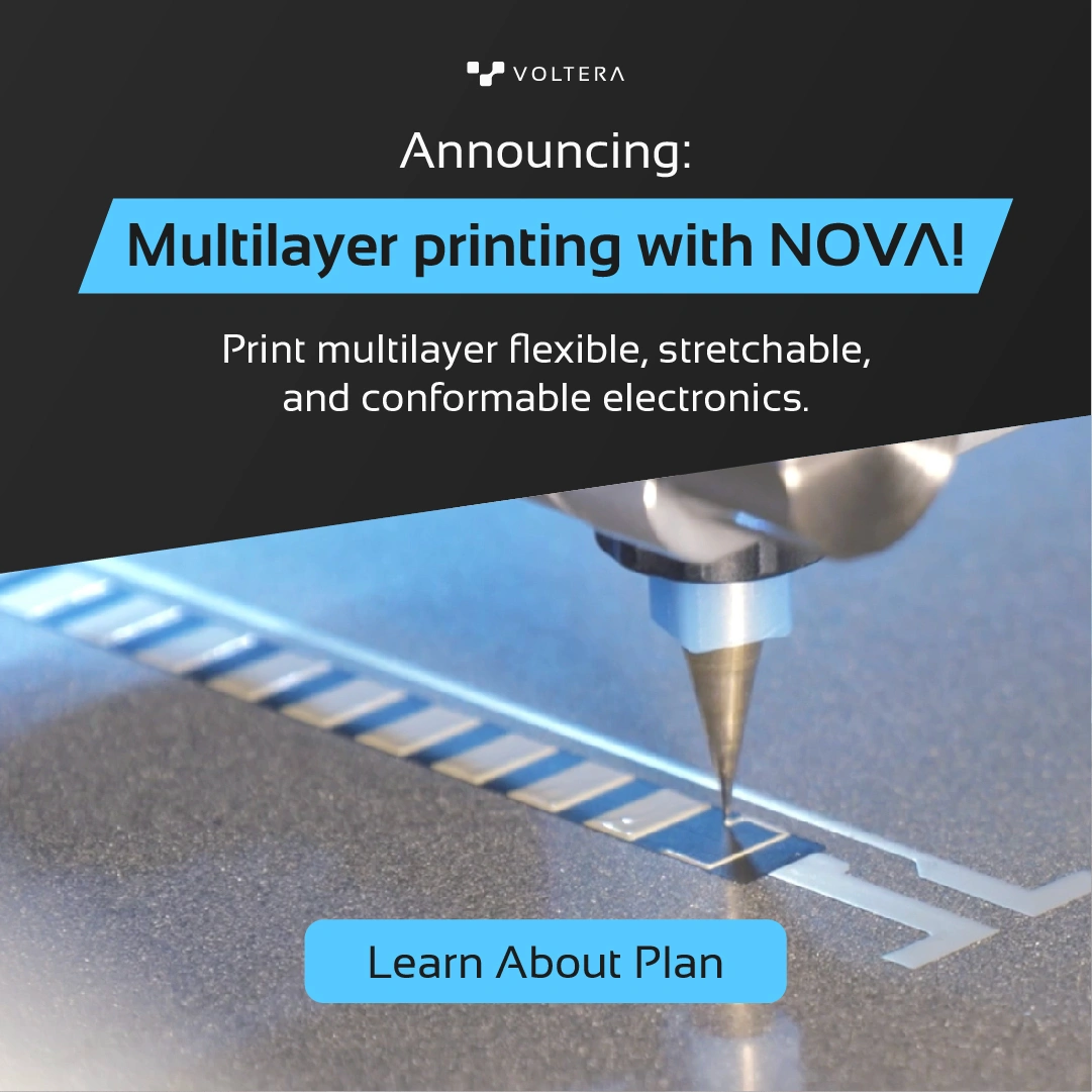
PCB prototyping supports various applications, including microcontrollers, sensors, integrated circuits (ICs), display devices, resistors, capacitors, and connectors. Additive PCB prototyping refers to prototyping PCBs using additive technologies — building circuits layer by layer using conductive inks and other materials.


APPLICABLE INDUSTRIES
- Consumer electronics
- Automotive
- Aerospace
- Healthcare
- Defense
COMMON MATERIALS
- Silver-based inks
- Carbon-based inks
- Solder paste
- Dielectric inks
- Silver-epoxy adhesives
COMMON SUBSTRATES
- FR1
- FR4
- PTFE (Teflon)
- Polyimide/Kapton
- Polyethylene terephthalate (PET)
- Ceramic
Our white papers
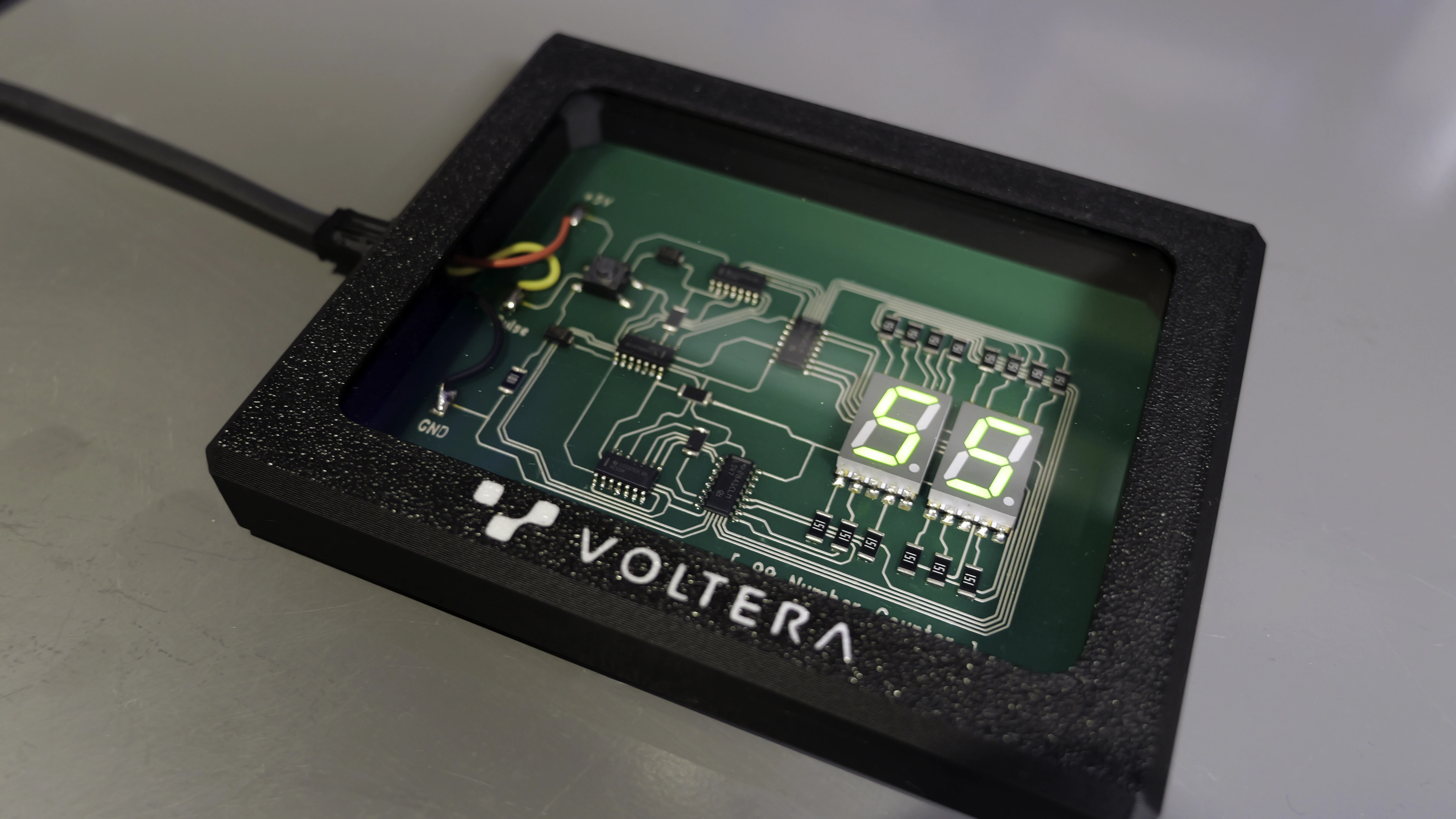
Printing a Decimal Counter Circuit with Silver Conductive Ink on FR1
Looking to go beyond breadboards? Read how we created a decimal counter with three interconnected circuits to teach the fundamentals of PCB development.
1
Next >2
Additional resources
Back to top